
Performance
According to the numerical results, a five-layer English letters X, Y, and Z pattern recognizer and a three-layer (0-1-2) MNIST handwritten digits classifier based on the presented on-chip programmable diffractive deep neural network architecture could achieve 100% and 91.86% prediction accuracies on the test dataset, respectively. FDTD testing of these structures reveals 98.8% and 92% matching with numerical testing results, respectively. Compared to the three-class pattern recognizer presented in7 for binary letter images with 15 pixels, which has numerical and FDTD testing accuracy of 98% and 95.8%, respectively, and a footprint of 450 μm×300 μm, the presented scheme has a much smaller footprint of 30 μm×40 μm for the 60-pixel pattern recognizer and 98 μm×21 μm for the more complex digits classifier, while showing comparable accuracies. It is also worth comparing our proposal to the three-class Iris flower classifier presented in8 with a footprint of 280 μm×1000 μm that has a numerical and experimental testing accuracy of 90% on the test dataset. Furthermore, both of those proposals7,8 are not programmable, and once fabricated, their Function is fixed and cannot be retrained for other Functions. A programmable multimodal scheme with 85.7% accuracy on multimodal (vision, audio, touch) test sets was previously presented in16, however, its footprint is very large (0.36 mm×1.42 mm). Moreover, the tunable diffractive units are implemented with thermo-optic phase shifters that are large-sized (3 μm×100 μm) and nonvolatile (which need a constant power supply to operate). Table 2 summarizes the characteristics of the previously presented on-chip diffractive optical neural networks and provides a comparison to the presented scheme in this article.
In the previous works based on direct-laser writing on Sb2Se3 thin film2,3, nonvolatile pixel perturbation patterns on a multimode interference device were optimized using an iterative method. Wu et al. employed a topology optimization approach to inverse-design the phase pattern of phase-change (Sb2Se3) multimode interference devices in a pixel-wise manner4. Adjoint optimization of on-chip phase-change (Sb2Se3) metasurfaces is a fast and efficient alternative optimization approach to those presented in2,3,4 to design phase change photonic devices. Furthermore, more complicated photonic devices with larger device areas can be designed. Other lithography-free reconfigurable demonstrations of on-chip photonic devices like photonic neural networks based on optical coding of spatial-temporal modulations of the imaginary index on an active III–V semiconductor platform17 and multimode interference power splitters based on plasma dispersion in planar silicon from all-optical excitation with spatially modulated pump beams18,19, although providing a convenient and cost-efficient paradigm for programmable integrated photonic circuits, suffer from a volatile nature. An on-chip programmable convolutional neural network based on a phase-change metasurface mode converter was also reported in20 by using phase-change material Ge2Sb2Te5 (GST). A photonic kernel with a 2 × 2 array of GST converters was experimentally demonstrated to perform MNIST handwritten (1–2) digits classification, which achieved experimental accuracy of 91% (91 out of 100 cases). However, the footprint of each GST converter is 80 μm×20 μm. Furthermore, the weight parameters are represented by 64 distinguishable levels created by partial phase transition of GST, which is rather difficult to implement.
The computational scale of many ONN architectures like integrated Mach-Zehnder interferometer grids, micro-ring modulator arrays, etc., is typically limited to 4 × 4 matrix-vector multiplications or smaller16. Therefore, most existing ONNs still struggle with classic tasks and small datasets like MNIST and Fashion-MNIST16. The on-chip diffractive optical neural networks, however, are supposed to enable large computational scales in the literature8,16. Our investigations indicate that these networks also are able to classify only 3–4 classes, suggesting fundamental limitations in their computational scale21. If the presented scheme in this article is benchmarked on the images of ten (0–9) handwritten digits from the MNIST dataset (for which the distance between two neighboring metasurfaces is 17 μm, the distance between the last metasurface and the output layer is 57 μm, the total device size is 98 μm×91 μm, and all other characteristics are similar to the ones presented in Table 1) the test accuracy and the FDTD matching score will be 76.02% and 30%, respectively. Therefore, Full 10-digit MNIST classification necessitates integration of 3 to 4 computing modules, each of which classifying 3 digits. More elaboration on the proposed hypothesis was presented in21, the summary of which is by increasing the classification categories, the classification accuracy of the on-chip diffractive optical neural networks degrades dramatically (e.g. for this scheme, the testing accuracy decreases from 91.86% for three classes to 76.02% for ten classes and matching score decreases from 92% for three classes to 30% for ten classes). Therefore, for the presented scheme, it can be deduced that the FDTD testing accuracy for ten (0–9) digits classification is about %76.02×%30 = 22.8%, which is rather a low classification accuracy. This consequence is signified when, for such neural networks, increasing the number of layers and/or the number of neurons per layer and/or changing the distance between the layers, don’t make a big difference in the classification accuracy, especially the FDTD testing accuracy21. These denote the limited capability of such a scheme to perform complex (multi-class) tasks21. As is described in21, the confusion matrices of many MNIST and Fashion-MNIST benchmarks with different numbers of classes reveal that these networks are able to classify only 3–4 classes correctly.
In the presented study, angular spectrum wave propagation that exploits fast Fourier transforms (FFTs) for formulating the diffraction is utilized to numerically simulate the on-chip programmable diffractive deep neural networks12,13. The numerical simulation results are verified using the 2.5D variational FDTD solver of the Lumerical Mode Solution. Despite very close matching between numerical simulation results and FDTD simulation results, a small discrepancy exists between them. This discrepancy is mainly justified by the differences in propagation models and discretization between diffraction-based modeling methods (like angular spectrum method) and full-wave electromagnetic modeling methods like FDTD.
The main challenge for the on-chip diffractive optical neural networks is the discrepancy between diffraction-based analysis methods and experimental/full-wave electromagnetic verifications. Many prior works7,8,9,21,22,23,24,25,26 tried to figure out the reason for this discrepancy. In this article, we add a few more analyses of such 2D structures to the former analyses. Figure 4 presents the results of these analyses. In Fig. 4, the performance of the (0-1-2) MNIST handwritten digits classifier with different numbers of metasurfaces (neural network layers) is investigated for different lattice constants of the phase-change metasurfaces. The lattice constant of the metasurfaces is set to 300 nm, 500 nm, and 700 nm in Figs. 4(a), 4(b), and 4(c), respectively. For these figures, the (aSb2Se3) rod width is fixed at 250 nm, 400 nm, and 600 nm, respectively, and the (aSb2Se3) rod length is selected as the learnable parameter. As is evident, while the testing accuracies are very near for the three lattice constants, the matching score between numerical and FDTD testing falls down by decreasing the lattice constant. Especially, for the more subwavelength 300 nm lattice constant (Fig. 4(a)), the matching score gets very low. In Fig. 4(d), the performance of the three-layer (0-1-2) MNIST handwritten digits classifier shown in Fig. 3 is studied when changing the operation wavelength. It is seen that the performance of the network remains nearly the same in the wavelength range of 1.5 μm to 1.6 μm, which indicates the broadband operation of the presented scheme. It should be mentioned that by increasing the wavelength, a slight decay in the testing accuracy as well as the matching score between the numerical and FDTD testing can be observed. This also indicates that a more subwavelength meta-atom results in a smaller matching score between numerical and FDTD testing. For the presented study in Fig. 4(d), the refractive index of Sb2Se3 between 1.5 μm and 1.6 μm is nearly constant27, and the refractive indices of silicon nitride and silicon oxide are extracted from28,29, respectively.
Fig. 4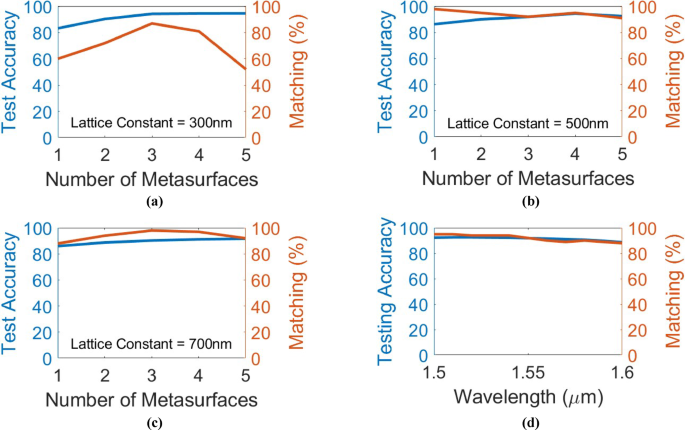
These figures illustrate how the subwavelength extent of phase-change metasurfaces affects the performance of the presented architecture. The blind testing accuracy for (0-1-2) MNIST handwritten digits classifier with different numbers of metasurfaces and the associated matching percentage between numerical testing and Lumerical 2.5D FDTD verification over 100 random images from the test dataset are shown for metasystems composed of (a) 300 nm-lattice constant phase-change metasurfaces, (b) 500 nm-lattice constant phase-change metasurfaces, and (c) 700 nm-lattice constant phase-change metasurfaces. (d) The blind testing accuracy and the matching percentage between numerical testing and Lumerical 2.5D FDTD verification over 100 random images from the test dataset, versus operation wavelength for the (0-1-2) MNIST handwritten digits classifier of Fig. 3.
Practical issues
For the presented on-chip optical neural network scheme, there might be a simulation-to-reality gap, as is also indicated in8 for the on-chip diffractive optical neural networks based on on-chip HCTA metasurfaces. This gap was attributed to the errors caused by the fabrication process in8, and an algorithm compensation method consisting of phase compensation and power compensation was exploited to reduce the negative impacts of errors. The phase compensation stage was implemented based on an online in-situ training procedure. Here, the rewritable nature of the on-chip optical neural network helps to easily perform the compensation stage. Furthermore, the whole training process of the on-chip optical neural network can be easily accomplished online and in situ by erasing and writing the diffractive units. In the context of on-chip diffractive optical neural networks, the presented programmable scheme can be a breakthrough, because it provides the opportunity to retrain these networks by in-situ training very easily. Direct laser writing technique makes it straightforward to adjust each neuron individually and therefore correcting the errors to restore the designed functionality1. Using the presented scheme and direct laser writing technique will assist finding the main reason for the limited scalability of these networks and if it is because of the incapability of Fourier-optics methods in modeling the evolution of optical fields through the network, then in-situ training would be an ideal solution for this problem.
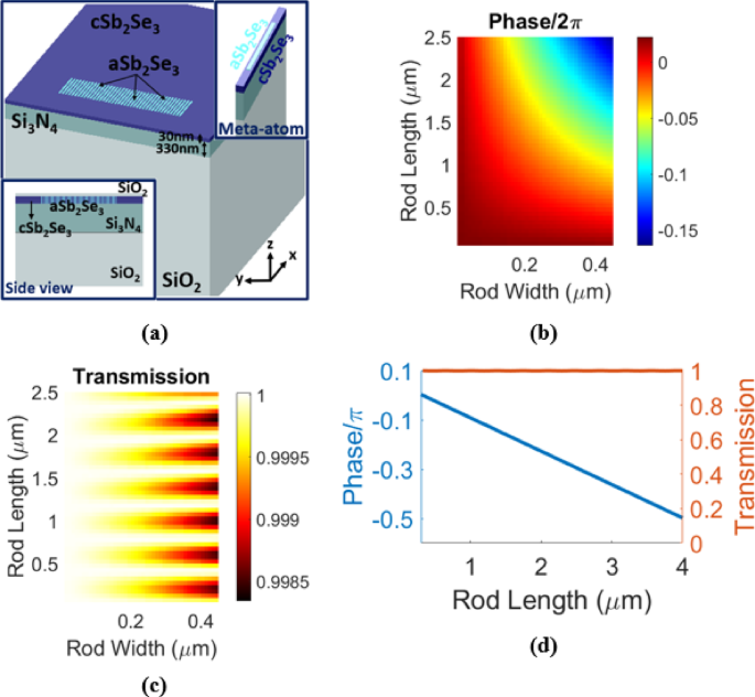
In our study, (aSb2Se3) rod array in the (cSb2Se3) thin film is considered as the phase-change metasurface. According to3, the method of direct laser writing of amorphous rods on a crystalline background leads to small pixels with well-defined edges. However, this can be achieved at the cost of much increased losses, as most of the Sb2Se3 layer is crystallized. On the other hand, for (cSb2Se3) rod array in the (aSb2Se3) thin film, direct laser writing of crystalline rods on an amorphous background offers limited spatial control over crystalline rods, generally resulting in larger rod size compared with amorphous rods3. In1, a commercial laser writing system (Heidelberg DWL 66+, 405-nm laser) was utilized to directly write the circuit layouts on a blank (cSb2Se3) thin film. The minimum achievable feature size with such an industrialized laser writing tool was 300 nm. In this article, for the presented on-chip programmable optical neural network designs to be complied with commercial laser writing constraints, the width of (aSb2Se3) rods is fixed at 400 nm, and the minimum value for (aSb2Se3) rods lengths is set to be 300 nm in the training processes. The thickness of the Sb2Se3 film is assumed to be 30 nm. As is mentioned in3, switching depths exceeding 200 nm are achieved for direct-write amorphization pulses in (cSb2Se3) thin films. Therefore, it is expected that 30 nm thickness to be in the regime where the entire thickness of the Sb2Se3 is switched.
As is indicated in3, losses stay very low for increasing thickness and length of Sb2Se3 in the amorphous state (in a waveguide). However, generally losses increase exponentially with the length of Sb2Se3 in both amorphous and crystalline states. While in3, these losses are attributed to surface and volume contributions, because of scattering by sidewall surface roughness and small poly-crystalline domains, Wu et al. considered the scattering induced by the grain boundaries within the (cSb2Se3) waveguide as the main source of loss1. According to1, the scattering loss can be mitigated when a lower erasure temperature is used to form larger crystal grains with sizes on the order of tens of micrometers. Based on3, the insertion loss over the device length dramatically reduces by decreasing the film thickness, however, larger Sb2Se3 film thickness leads to increased modulation per Sb2Se3 film length. As a result, due to1,3, a 30 nm-thickness Sb2Se3 film will have a propagation loss between (0.003–0.01) dB/µm, which is rather negligible, considering the small propagation lengths in the presented schemes.
According to3, thicker Sb2Se3 layers can provide an increase in the induced optical phase shift of each neuron ((aSb2Se3) rod), however, this is achieved at the cost of increased losses by absorption, scattering, and multimode contributions. Figures 5(a), 5(b), and 5(c) show the performance of an MNIST (0-1-2) digit classifier with different numbers of metasurfaces (hidden layers) for the (cSb2Se3) film thicknesses of 30 nm, 70 nm and 100 nm, respectively. A slight improvement in the matching score between analytical testing and 2.5D FDTD testing is observed. For (cSb2Se3) film thicknesses of 70 nm and 100 nm, the (aSb2Se3) rods’ lengths vary in the range [300 nm, 2 μm], as this range provides more than π/2 phase shift for each neuron ((aSb2Se3) rod). The (cSb2Se3) film losses are not taken into account in these investigations because of the lack of approximate loss values for these thicknesses in previous studies1,4. The loss values presented in3 were measured for Sb2Se3 films with different thicknesses deposited on silicon (SOI platform), which differs from the Si3N4-on-insulator platform used in this study. However, the losses are expected to be negligible due to the small propagation distance of 21 μm in this network.
Also, it can be deduced from Fig. 5 that increasing the number of metasurfaces in the network generally results in a higher numerical accuracy. However, while the matching score exists very high for most of the instances, its variations seem to follow a random trend with increasing the number of layers. Therefore, it can be concluded that increasing the number of metasurfaces slightly improves the performance for this scheme. This trend was also observed for X-Y-Z letter recognition in the related investigations. But it depends on the task and cannot be generalized to all tasks.
Fig. 5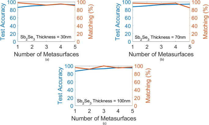
These figures illustrate how the phase-change film thickness affects the performance of the presented (0-1-2) MNIST handwritten digits classifier. The blind testing accuracy of the classifier with different numbers of metasurfaces and the associated matching percentage between numerical testing and Lumerical 2.5D FDTD verification over 100 random images from the test dataset are shown for (cSb2Se3) film thicknesses of (a) 30 nm, (b) 70 nm, and (c) 100 nm.
Fig. 6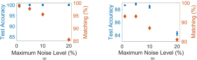
These figures illustrate how noisy input affects the performance of the presented scheme trained for (a) X-Y-Z pattern recognition, (b) (0-1-2) MNIST handwritten digits classification. The blue markers indicate the blind testing accuracy of the network over the test dataset, and the red markers indicate the matching score between numerical testing and Lumerical 2.5D FDTD verification over 90 and 100 random images from the test dataset for X-Y-Z pattern recognition and (0-1-2) MNIST handwritten digits classification, respectively. The error bars in (b) show the results for three testing experiments.
According to maximum propagation loss (4.5 dB/mm) that was mentioned in1 for photonic integrated circuits, the simulations are repeated with (cSb2Se3) extinction coefficient equal to \(k=2.5561 \times {10^{ – 4}}\). The matching score between numerical testing and FDTD testing remains the same as the system without loss for X-Y-Z pattern recognizer (98.8%) and MNIST (0-1-2) digits classifier (92%). Also, the performance is investigated for the extinction ratio of \(k={10^{ – 3}}\) that is equivalent to an approximate propagation loss of 17.6 dB/mm, and the performance remains the same for both X-Y-Z pattern recognizer and MNIST (0-1-2) digits classifier.
It should be mentioned that the presented scheme is mainly applicable to reprogrammable devices that don’t necessarily require very fast switching, and a Sb2Se3 endurance of thousands to millions of cycles is sufficient for them2,3. Further improvements in the surrounding materials’ thermal design and integration into highly optimized device configurations can substantially improve switching speed and endurance2,3.
Finally, our simulations show that the system is able to tolerate noisy or imperfect input encoding. Figure 6 shows the results of these simulations. In the simulations, random noise is applied to the input images. The applied maximum noise levels are [1%, 5%, 10%, 20%] of the maximum signal level. The testing accuracy on the test set remains 100% for all noise levels in X-Y-Z pattern recognition, and the matching score modifies to [98.8%, 97.7%, 95.5%, 85.5%] (Fig. 6(a)). The testing accuracy on the test dataset drops from 91.86% to [88.62%, 88.87%, 88.40%, 84.23%] for MNIST (0-1-2) dataset (Fig. 6(b)). The error bars show the results for three testing experiments. The matching score changes from 92% to [93%, 93%, 87%, 81%].