
Design of the reconfigurable non-Abelian photonic chip
Figure 1a illustrates a schematic diagram of the proposed reconfigurable non-Abelian photonic chip, which is double-layered and mainly consists of four single-mode polymer waveguides A, B, C, and D (gray) located in layer II. The photonic chip is designed to realize the non-Abelian braiding of these four modes, i.e., the output and input of the chip are associated with a non-Abelian holonomy induced geometric phase matrix belonging to the braid group B443. To achieve this goal, some auxiliary waveguides (blue) and coupling waveguides (red) are introduced in layers I and II, respectively. At specific regions, electrode heaters (yellow) are placed on top of layer II, which can be exploited to tune the refractive index of the braiding waveguides (i.e., A, B, C, or D) and thus the braiding-induced geometric phase matrix. The chip consists of six sets of tunable two-mode braiding structure, which acts as building blocks.
Fig. 1: Schematic diagram of a reconfigurable non-Abelian photonic chip.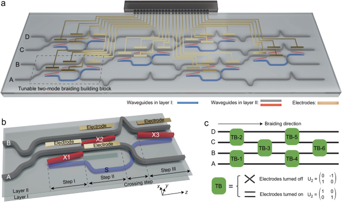
a Schematic diagram of a double-layered polymer photonic chip which performs the task of non-Abelian braiding of four photonic modes located in waveguides A to D (gray), respectively, with the assistance of several auxiliary waveguides (blue) and coupling waveguides (red). The chip consists of six two-mode braiding structures as building blocks (dashed region), where electrode heaters (yellow) are introduced on top of the braiding waveguides to tune their refractive index via the thermo-optic effect. b An enlarged view of one building block, where an auxiliary waveguide (S) is placed in layer I, while braiding waveguides (A and B) and coupling waveguides (X1, X2, and X3) are located in layer II. The whole two-mode braiding process can be divided into steps I, II, and III, plus a crossing step for the repositioning of the waveguides. When electrode heaters are turned off, the braiding results in a swap of the two modes in waveguides A and B via a non-Abelian holonomy process. When electrode heaters are turned on, the refractive index of the braiding waveguides is significantly lowered down, leading to that the output and input are in the same braiding waveguide. c A braiding diagram of the photonic chip, where each green box represents a tunable two-mode braiding building block. The abbreviation “TB” is short for tunable block, which has two working conditions associated with two geometric phase matrices U2, depending on the modulation. By separately tuning the six TBs, a variety of unitary matrices associated with the braid group B4 can be achieved in this single chip.
We study the physical mechanism of the chip by focusing on the tunable braiding building block. Figure 1b shows an enlarged view of one building block (i.e., the one enclosed by the dashed line in Fig. 1a) where two modes in waveguides A and B are braided. These two braiding waveguides, together with three coupling waveguides, namely X1, X2, and X3, are in layer II, while an auxiliary waveguide S is placed below them in layer I. The interlayer distance is 5.4 μm, and all the waveguides share the same rectangular cross section of 4.5 × 4 μm2. Apart from the input region, the process that light propagates in the building block can be mainly divided into three steps, while there is a crossing step between steps II and III for the repositioning of the waveguides. Since the refractive index contrast between the waveguide and the cladding is ~0.0144, light propagating in the paraxial waveguides can be described by a Hamiltonian
$$H\left(z\right)=\left[\begin{array}{cccc}{\beta }_{{{\rm{X}}}}(z) & {\kappa }_{{{\rm{AX}}}}(z) & {\kappa }_{{{\rm{BX}}}}(z) & {\kappa }_{{{\rm{SX}}}}(z)\\ {\kappa }_{{{\rm{AX}}}}(z) & {\beta }_{{{\rm{A}}}}(z) & 0 & 0\\ {\kappa }_{{{\rm{BX}}}}(z) & 0 & {\beta }_{{{\rm{B}}}}(z) & 0\\ {\kappa }_{{{\rm{SX}}}}(z) & 0 & 0 & {\beta }_{{{\rm{S}}}}(z)\end{array}\right],$$
(1)
where \({\kappa }_{{{\rm{AX}}}}\), \({\kappa }_{{{\rm{BX}}}}\) and \({\kappa }_{{{\rm{SX}}}}\) denote the position-dependent coupling strength between waveguides A, B, S, and Xi in the ith step (i = 1, 2, 3), respectively, and \({\beta }_{{{\rm{A}}}}\), \({\beta }_{{{\rm{B}}}}\), \({\beta }_{{{\rm{S}}}}\) and \({\beta }_{{{\rm{X}}}}\) are the propagation constant of the fundamental mode in the corresponding waveguides.
We first consider the situation that the electrode heaters are turned off. In this case, the diagonal terms of the Hamiltonian are constants, i.e., \({\beta }_{{{\rm{A}}}}\left(z\right)={\beta }_{{{\rm{B}}}}\left(z\right)={\beta }_{{{\rm{S}}}}\left(z\right)={\beta }_{{{\rm{X}}}}\left(z\right)={\beta }_{0}\), leading to a braiding result that the two modes in waveguides A and B are swapped. We focus on the wavelength of 1550 nm and show the fitted coupling coefficients in the upper panel of Fig. 2a (see Supplementary Note 1 and Supplementary Fig. 1 for fitting details). By enforcing this Hamiltonian with chiral symmetry13,19, the system supports four eigenmodes, as shown by their propagation constants in the lower panel of Fig. 2a. Among them, two photonic “zero” modes with \({\beta=\beta }_{0}\) are degenerate, forming a degenerate subspace in which the braiding takes place. The whole braiding process can be interpreted as follows. At step I, the waveguides A, X1, and S are coupled via a stimulated Raman adiabatic passage45, leading to a complete energy transfer from the waveguide A in layer II to S in layer I, in the form of a photonic “zero” mode. Meanwhile, the waveguide B is isolated so that a “zero” mode injected there remains there. Steps II and III follow the same principle. At step II, the waveguides A, X2, and B in the same layer II are so coupled to pump a “zero” mode from waveguide B to A, while the waveguide S is uncoupled. At step III, a “zero” mode is adiabatically transferred from the waveguide S to B with the help of X3, while another “zero” mode in waveguide A is isolated. The building block then accomplishes the task of two-mode braiding, i.e., the two injected modes in waveguides A and B are swapped. Figure 2b, c shows the calculated light intensity distributions in the building block when light is injected in the waveguides A and B, respectively, by employing a 3D finite-difference beam propagation method (RSoft 3DFD-BPM). The light trajectory and mode conversion behavior are in accordance with the above analysis.
Fig. 2: Physics of the tunable two-mode braiding building block.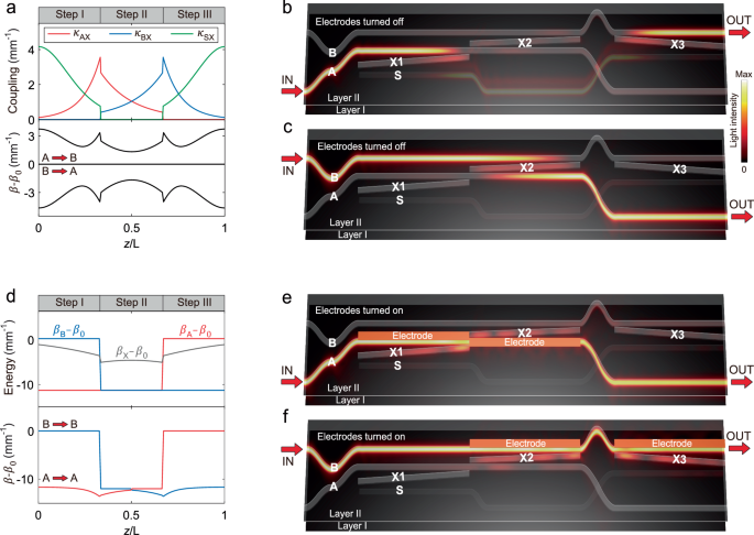
a The fitted coupling coefficients between adjacent waveguides (upper panel) and the calculated propagation constants \(\beta\) (lower panel) in the two-mode braiding building block when electrode heaters are turned off. The non-Abelian holonomy occurs following the flat band with \({\beta=\beta }_{0}\), resulting in a swap of the two modes supported in waveguides A and B. The simulated light intensity distributions in the two-mode braiding building block with electrodes turned off, when the input is via the waveguide A (b) and B (c). d The fitted diagonal terms of the Hamiltonian (upper panel) and the calculated propagation constants \(\beta\) (lower panel) in the two-mode braiding building block when the electrode heaters are turned on. Following the red and blue bands, a mode remains in the same waveguide where it is injected. The simulated light intensity distributions in the two-mode braiding building block with electrodes turned on, when the input is via the waveguide A (e) and B (f).
These two processes exactly follow the double-degenerate flat band in Fig. 2a. Since the bending parts in waveguides A, B and S in the whole braiding process (including the crossing step) are judiciously designed to ensure that these three waveguides share the same total length, the two accumulated dynamical phases in the two braiding processes with “zero” modes are the same. In contrast, the non-Abelian holonomy gives rise to different geometric phases obtained in the two braiding processes. They are related to the off-diagonal terms of a 2 × 2 geometric phase matrix that can be calculated via \({U}_{2}={{\mathcal{P}}}\exp \left(i\int {A}_{{mn}}(\lambda )d\lambda \right)\{m={1,2},n={1,2}\}\), with \(\lambda\) and \({{\mathcal{P}}}\) being the evolution path and order, respectively, and \({A}_{{mn}}\left(\lambda \right)=i{{\langle }}{\psi }_{m}\left(\lambda \right)|{\partial }_{\lambda }|{\psi }_{n}\left(\lambda \right){{\rangle }}\) is the Berry connection matrix15. For this two-mode braiding, the geometric phases when injecting light in A and B are 2π and π, respectively. This leads to \({U}_{2}=\left[\begin{array}{cc}0 & -1\\ 1 & 0\end{array}\right]\) that satisfies \({U}_{2}|{\psi }_{{{\rm{A}}}}{{\rm{\angle }}}={|\psi }_{{{\rm{B}}}}{{\rm{\angle }}}\) and \({U}_{2}|{\psi }_{{{\rm{B}}}}{{\rm{\angle }}}=-|{\psi }_{{{\rm{A}}}}{{\rm{\angle }}}\) where \(|{\psi }_{{{\rm{A}}}}{{\rm{\angle }}}={[{\mathrm{1,0}}]}^{{{\rm{T}}}}\) and \({|\psi }_{{{\rm{B}}}}{{\rm{\angle }}}={[{\mathrm{0,1}}]}^{{{\rm{T}}}}\) are the eigenfunctions of the modes in waveguide A and B, respectively.
We turn to the situation that the electrode heaters are turned on. In this case, the braiding is avoided, meaning that the input and output are in the same waveguide (A or B). To realize this, four rectangular electrode heaters with a thickness of ~200 nm are used to tune the building block (see Fig. 1b). Two out of them are placed on top of the waveguide A at steps I and II, while the other two are put on top of the waveguide B at steps II and III. The refractive index of the waveguide and cladding adjacent to the electrode is significantly lowered down since the polymer material has a large thermo-optic coefficient of approximately −1 × 10⁻⁴/K (see Supplementary Fig. 2 for the induced refractive index distributions). As a result, the propagation constant of those waveguides near the electrode is no longer a constant. The upper panel in Fig. 2d shows the calculated heating-induced position-dependent diagonal terms of the Hamiltonian. We find that as expected, \({\beta }_{{{\rm{A}}}}\left(z\right)\) and \({\beta }_{{{\rm{B}}}}\left(z\right)\) at steps with electrodes are greatly changed, while \({\beta }_{{{\rm{X}}}}\left(z\right)\) is affected slightly. Since the waveguide S is sufficiently far away from the electrodes, \({\beta }_{{{\rm{S}}}}\left(z\right)={\beta }_{0}\) still holds (not represented in Fig. 2d). Although the off-diagonal terms (i.e., coupling strengths) are almost the same as those in Fig. 2a, the large detuning introduced in waveguides A and B associated with the diagonal terms can greatly change the eigenvalues of the Hamiltonian and thus the light transmission behavior, as the chiral symmetry is broken (see Supplementary Note 2 for a detailed theoretical analysis). The lower panel in Fig. 2d shows the calculated propagation constants of the two modes associated with waveguides A (red) and B (blue). We note that the original degenerate flat band is split into two nondegenerate bands with electrodes turned on, following which the light transportation remains in the same waveguide. This can be verified by Fig. 2e, f, which represents the calculated light intensity distributions with input in the waveguides A and B, respectively. We emphasize that the accumulated dynamical phases in these two processes are still the same, since the two bands are symmetric with respect to the center. Obviously, no geometric phase is obtained in this case, which leads to \({U}_{2}=\left[\begin{array}{cc}1 & 0\\ 0 & 1\end{array}\right]\). We also calculate the wave transmission by directly using the fitted Hamiltonian, and the results (see Supplementary Fig. 3) are found to match well with those in Fig. 2b, c, e, f.
After demonstrating the working mechanism of the tunable two-mode braiding building block, the reconfigurable functionality of the chip is easy to understand. Figure 1c shows a simplified schematic of the four-mode braiding chip, where each green box represents a tunable building block that has two working conditions and associated geometric phase matrices. By separately tuning these building blocks, a variety of unitary matrices associated with the braid group B4 can be realized in the same photonic chip. In what follows, we will experimentally demonstrate up to 24 unitary matrices that exactly form a permutation group S4.
Experimental demonstration of the two-mode braiding building block
We fabricated the double-layered photonic chip using spin-coating, photolithography, and wet-etching processes in sequence (see Methods and Supplementary Fig. 4 for details). To characterize the modulation performance, we first fabricated three devices containing only steps I, II, and III of the building block, respectively (see Supplementary Fig. 5 for microscope images of the sample). The corresponding measured output light intensity images when a single waveguide was launched by a laser at 1550 nm (see the red arrows) are shown in Fig. 3a–c, respectively. We note that when the waveguide A is injected at step I (Fig. 3a), light exits mainly via the waveguide S with electrodes turned off, while it remains in the waveguide A by turning on the electrode heaters. At step II (Fig. 3b), a “zero” mode is adiabatically pumped from the waveguide B to A when the electrodes are turned off. By turning on them, in contrast, the mode remains in the injected waveguide (either A or B). At step III (Fig. 3c), the same phenomenon regarding the modulation occurs between the waveguides S and B.
Fig. 3: Experimental demonstration of the tunable two-mode braiding building block.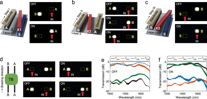
a Measured output light intensity images of a structure featuring only step I with a laser of 1550 nm injected from the waveguide A, when the electrode heaters are turned off (upper panel) and on (lower panel). b Measured output light intensity images of a step II structure, where the input is from the waveguide B with electrodes turned off (upper panel), from the waveguide B (middle panel), or A (lower panel) with electrodes turned on. c Measured output images of step III, where light is injected from the waveguide S with electrodes turned off (upper panel) and from the waveguide B with electrodes turned on (lower panel). d Measured output light intensity images of the two-mode braiding structure when the electrode heaters are turned off (left column) and on (right column). In (a–d), the red arrows mark the waveguide in which light is injected. Measured transmission coefficients TA,A, TB,A, TA,B, and TB,B (see main text for definition) in the two-mode braiding building block as a function of wavelengths when the electrode heaters are turned off (e) and on (f).
Since the three structures related respectively to the three steps work well, we combined them and fabricated a two-mode braiding building block. The experimentally measured output patterns at 1550 nm are shown in Fig. 3d. As expected, the output and the input are located in different waveguides with electrodes turned off, while they are in the same waveguide when all the electrode heaters are turned on. The applied driving power for each electrode heater is ~120 mW. The switching exhibits a response time of ~1 ms, primarily attributed to the low thermal conductivity inherent to polymer materials. The response time of the device can be further improved by employing the polymer/silica hybrid waveguide structure46.
We emphasize that since the braiding is a non-resonant effect which is protected by the system topology in Hilbert space, the geometric phase matrix and mode switching phenomenon are robust and apply to broadband wavelengths. To demonstrate this point, we measured the transmission coefficient Tj,i, defined as the light transmission from an input waveguide i to an output waveguide j {i,j = A,B}, in the wavelength range of 1500–1630 nm. The measured results by excluding the insertion loss and outcoupling effects are given in Fig. 3e, f, for the case when electrode heaters are turned off and on, respectively. We note that for the former case, the transmission coefficient TB,A (TA,B) is significantly higher than the crosstalk TA,A (TB,B) in the whole wavelength range of interest, with an average extinction ratio of ~17.2 dB (~14.4 dB). The situation is reversed when the electrode heaters are turned on, where the transmission coefficient TA,A (TB,B) is larger than the crosstalk TB,A (TA,B), with an average extinction ratio of ~17.8 dB (~14.2 dB). These experimental results clearly demonstrate the broadband feature of the proposed tunable two-mode braiding building block. As the multi-mode braiding device is consisted of multiple two-mode braiding building blocks, the proposed photonic chip can also work in broadband, as long as the waveguide fundamental mode is well supported in the wavelength of interest. A systematic study on the broadband and robust features is provided in Supplementary Note 3 and Supplementary Figs. 6−10.
Experimental demonstration of reconfigurable multi-mode non-Abelian braiding devices
The tunable building blocks can be cascaded to realize reconfigurable non-Abelian braiding of multiple photonic modes. We first take a three-mode non-Abelian braiding as example (see Supplementary Fig. 11 for the structure) and show the braiding diagram and experimentally measured output patterns of light intensity at the wavelength of 1550 nm in Fig. 4a–f. The device consists of three tunable blocks namely TB-1, TB-2 and TB-3. Figure 4a shows the case that all the electrode heaters are turned off. In this case, a mode injected from the waveguide A, B and C exits the device via the waveguides C, B and A, respectively, leading to a geometric phase matrix \({U}_{3}=\left[\begin{array}{ccc}0 & 0 & 1\\ 0 & -1 & 0\\ 1 & 0 & 0\end{array}\right]\) that connects the input and output via \(|{\psi }_{{{\rm{OUT}}}}{{\rm{\angle }}}={U}_{3}|{\psi }_{{{\rm{IN}}}}{{\rm{\angle }}}\), with the input \(|{\psi }_{{{\rm{IN}}}}{{\rm{\angle }}}\) being \(|{\psi }_{{{\rm{A}}}}{{\rm{\angle }}}={[{\mathrm{1,0,0}}]}^{{{\rm{T}}}}\), \(|{\psi }_{{{\rm{B}}}}{{\rm{\angle }}}={[{\mathrm{0,1,0}}]}^{{{\rm{T}}}}\) or \(|{\psi }_{{{\rm{C}}}}{{\rm{\angle }}}={[{\mathrm{0,0,1}}]}^{{{\rm{T}}}}\). By exerting modulations, the proposed device can be reconfigured to realize various geometric phase matrices belonging to the braid group B3. Figure 4b–d shows the cases that only the TB-1, TB-2 or TB-3 is turned on, where the geometric phase matrix is correspondingly changed to be \(\left[\begin{array}{ccc}0 & -1 & 0\\ 0 & 0 & -1\\ 1 & 0 & 0\end{array}\right]\), \(\left[\begin{array}{ccc}1 & 0 & 0\\ 0 & -1 & 0\\ 0 & 0 & -1\end{array}\right]\) or \(\left[\begin{array}{ccc}0 & 0 & 1\\ 1 & 0 & 0\\ 0 & 1 & 0\end{array}\right]\), respectively. When the TB-1 and TB-2 are simultaneously turned on, a geometric phase matrix \({U}_{3}=\left[\begin{array}{ccc}1 & 0 & 0\\ 0 & 0 & -1\\ 0 & 1 & 0\end{array}\right]\) is obtained (Fig. 4e). Another configuration \({U}_{3}=\left[\begin{array}{ccc}0 & -1 & 0\\ 1 & 0 & 0\\ 0 & 0 & 1\end{array}\right]\) can be accessed by simultaneously turning on the TB-1 and TB-3 (Fig. 4f). When considering the mode switching behavior only (that is, without the phase information), the above six group elements in Fig. 4a–f form a permutation group S3. The corresponding geometric phase matrices for each case are summarized in Supplementary Table 1.
Fig. 4: Experimental demonstration of a reconfigurable three-mode non-Abelian braiding device.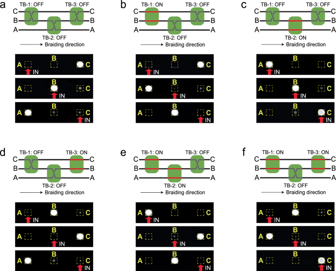
a Measured output light intensity images of a reconfigurable three-mode non-Abelian braiding device consisting of three TBs at 1550 nm, when all the TBs are turned off. b–f Experimental results of the three-mode non-Abelian braiding device when some of the TBs are turned on (see the braiding schematic for details). The red arrows mark the waveguide in which light is injected.
The principle can be expanded to achieve the reconfigurable non-Abelian braiding of more photonic modes. We come back to the four-mode non-Abelian braiding photonic chip illustrated in Fig. 1a. The braid group B4 has three generators: \({\sigma }_{1}\), \({\sigma }_{2}\), and \({\sigma }_{3}\), which can be realized using a two-mode braiding building block with waveguides A and B (see Fig. 1b), B and C, and C and D, respectively. With these definitions, the group element representing the reconfigurable device in Fig. 1a is given by \({({\sigma }_{1})}^{{n}_{1}}{({\sigma }_{3})}^{{n}_{2}}{({\sigma }_{2})}^{{n}_{3}}{({\sigma }_{1})}^{{n}_{4}}{({\sigma }_{3})}^{{n}_{5}}{({\sigma }_{2})}^{{n}_{6}}\), where each \({n}_{i}\in \{{\mathrm{0,1}}\}\) depends on whether the corresponding electrode heater TB-i is turned on (\({n}_{i}=0\)) or off (\({n}_{i}=1\)). In this way, our device can be reconfigured to realize a total of 26 = 64 settings of braiding operations. In our experiment, we choose 24 settings out of them by turning on at most three sets of electrode heaters simultaneously. These 24 unitary transformations also form a permutation group S4. Figure 5 shows the experimentally measured light output patterns of 9 settings by exerting different modulations (see the inset for details), while the experimental results for the other 15 settings where one, two and three building blocks are turned on, are given in Supplementary Figs. 12–14, respectively. The corresponding geometric phase matrices for each case are given in Supplementary Table 2.
Fig. 5: Experimental demonstration of a reconfigurable four-mode non-Abelian braiding device.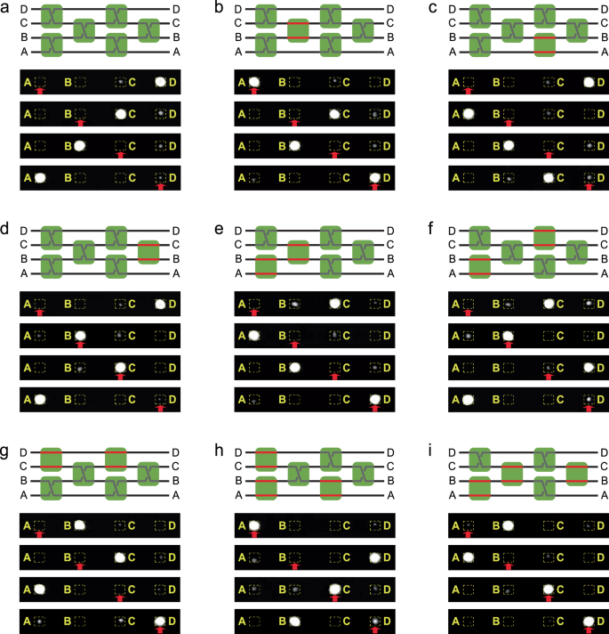
a–i Measured output light intensity images of a reconfigurable four-mode non-Abelian braiding device consisting of six TBs at 1550 nm, when some of the TBs are turned on (see the braiding schematic for details). The red arrows mark the waveguide in which light is injected. These results, together with the experimental results in Supplementary Figs. 12–14, demonstrate that the device can be reconfigured to achieve a fruitful set of four-mode non-Abelian braiding.
The braid group B4 is an infinite group, and a general element can be written as \({({\sigma }_{1})}^{{n}_{1}}{({\sigma }_{2})}^{{n}_{2}}{({\sigma }_{3})}^{{n}_{3}}{({\sigma }_{1})}^{{n}_{4}}{({\sigma }_{2})}^{{n}_{5}}{({\sigma }_{3})}^{{n}_{6}}\ldots\), where \({n}_{i}{\mathbb\,{\in }}{\mathbb\,{Z}}\). A universal solution could be a reconfigurable device in which six tunable building blocks associated with the six basic braids of the group are cascaded in sequence, i.e., \({\sigma }_{1}\), \({\sigma }_{1}^{-1}\), \({\sigma }_{2}\), \({\sigma }_{2}^{-1}\), \({\sigma }_{3}\), and \({\sigma }_{3}^{-1}\), where the inverse braids (i.e., \({\sigma }_{1}^{-1}\), \({\sigma }_{2}^{-1}\), \({\sigma }_{3}^{-1}\)) can be realized by simply reversing the device structure of Fig. 1b along the x axis. By controlling the array of electrode heaters according to the values of \({n}_{i}\) and repeatedly feeding back the output of the device to the input in situ using auxiliary circuits (see Supplementary Fig. 15 for a schematic), the reconfigurable non-Abelian braiding device can in principle realize any element associated with the braid group B4. In addition, by adding or removing necessary working waveguides (i.e., gray ones in Fig. 1a), a reconfigurable braiding belonging to a general braid group Bi can also be achieved. These results and outlook demonstrate the scalability and versatility of the proposed reconfigurable approach.
At last, we discuss how to eliminate the dynamical phase effect in the reconfigurable non-Abelian braiding process. In the design in Fig. 1a, we have introduced various bending to the braiding waveguides A to D, to guarantee that they share the same total length (see Supplementary Fig. 16 for details). In this sense, the accumulated dynamical phase for each working mode is solely related to the propagation constant, which is always equal to \({\beta }_{0}\) except in the building block with electrodes turned on (see Fig. 2d). To tackle such difference, one can introduce an extra electrode heater for each braiding waveguide after each braiding step. By turning on specific electrode heaters, the difference of the dynamical phase accumulation in different braiding waveguides could be compensated (see Supplementary Fig. 17 for details).