
Birefringence in cubic MAPbBr3
Our investigation begins with the observation of an unexpected optical anisotropy in the room-temperature phase of MAPbBr3. Similar to other LHPs, the basic structure of MAPbBr3 is composed of corner-sharing BX6 (Fig. 1a) octahedra, forming transparent rectangular-shaped crystals with a nominally cubic symmetry above \(T\) ≈ 230 K26. However, a careful study of generic crystals demonstrates this is not the case in general. Fig. 1b shows a typical pristine MAPbBr3 crystal grown from solution by inverse temperature crystallization7. To examine its optical properties, the crystal was placed in a rotating crossed-polarizer setup (Fig. 1c) and illuminated by a 632.8 nm He-Ne laser beam normal to the (001) plane, while varying the angle of polarization relative to the [100] crystal axis (Methods). The rotation of the crossed polarizer was captured on video (Supplementary Movie 1). Fig. 1d shows transmitted light images of the MAPbBr3 crystal, illuminated with light polarized at 0° and 45°, respectively, revealing its complex birefringent structure. This is an unexpected observation, as MAPbBr3 is expected to be in a cubic phase at room temperature26, which is incompatible with the observed birefringence. This definitively indicates that the crystal symmetry of the MAPbBr3 sample is lower than the nominal \({Pm}\bar{3}m\) space group. While the birefringence of nominally cubic MAPbBr3 is commonly observed, this incongruity is not systematically addressed in the literature. It is typically attributed to the inferior quality of the solution-processed crystals27, but the exact nature of this symmetry lowering remains to be understood.
Fig. 1: Birefringence in the nominally cubic high-temperature phase of MAPbBr3.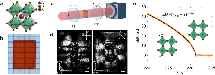
a Crystal structure of cubic perovskite with the general chemical formula ABX3. b A typical MAPbBr3 crystal grown from solution using the inverse temperature crystallization technique. c Schematic of the crossed-polarizer setup used to visualize the birefringence in the high-temperature phase of MAPbBr3. d Polarized light images of the MAPbBr3 sample shown in Fig. 1b placed between crossed polarizers oriented at 0° and 45° relative to the [100] crystal axis. The scale bars are 500 µm. e Cumulative phase retardation \(\triangle \varTheta\) as a function of temperature across the cubic-to-tetragonal phase transition in MAPbBr3 single crystal. The solid black line represents the best fit to the data above the nominal critical temperature \({T}_{{{{\rm{c}}}}}\) = 231.2 °C of the form \(\Delta \varTheta \propto {\left|{T}_{{{{\rm{c}}}}}-T\right|}^{\alpha }\). The goodness-of-fit is \({R}^{2}\) > 0.999. Inset images show the tilting pattern of PbBr6 octahedra associated with the phase transition.
The cubic-to-tetragonal transition in MAPbBr3 is identified as a close-to-second-order first-order displacement-type phase transition driven by the rotation of BX6 octahedra21,28 (see inset to Fig. 1e). Reflecting the structural change, the electric susceptibility tensor is also modified at the phase transition, which is manifested in the corresponding change in the optical refractive index ellipsoid. Birefringence, therefore, provides information on the onset of phase transition and can be used as an indicator of the order parameter of the phase transition. X-ray diffraction studies revealed that the order parameter of the cubic-to-tetragonal phase transition in MAPbBr3 is the rotation angle of the PbBr6 octahedra21. The idea that the same order parameter drives the formation of the distorted cubic phase at room temperature seemed plausible, which is why we proceeded with measuring the temperature dependence of birefringence across the phase transition. The critical behavior was evaluated by measuring the temperature dependence of the Stokes parameters of a polarized near-infrared beam passing through the MAPbBr3 crystal placed inside the cryostat (Methods, Supplementary Fig. 1, Supplementary Note 1), and fitting the cumulative phase retardation acquired by the beam to a power law \(\Delta \varTheta \propto {\left|T-{T}_{{{{\rm{c}}}}}\right|}^{\alpha }\) (Fig. 1e). As can be seen in the figure, the temperature dependence of birefringence retains the sharp anomaly at \({T}_{{{{\rm{c}}}}}\), with high-temperature birefringence providing a simple offset to the critical birefringence associated with the phase transition. This indicates that the symmetry lowering of MAPbBr3 at room temperature has a nature distinct from the low-temperature rotation of PbBr6 octahedra in the tetragonal phase.
Microscopic structure of local anisotropy in MAPbBr3
A birefringent sample can appear dark when placed between two orthogonally crossed polarizers only if the polarization axis of one of the polarizers matches the optical axis of the sample. In contrast, an optically active sample will always appear bright, while an isotropic sample will always be dark. Our optical measurements showed that no part of the sample remains permanently bright or dark for all orientations of the mutually crossed polarizers relative to the crystal axes (Supplementary Movie 1). The data indicate that the sample is birefringent everywhere, with no optical activity, and with locally defined optical axes seemingly uncorrelated with crystal directions.
Birefringence in a nominally cubic system indicates the presence of bulk strain. In a free-standing crystal, inhomogeneous strain implies the presence of defects, such as dislocations, or, in the case of spontaneous strain (ferroelasticity), domain boundaries29. To investigate the nature of nonuniform strain in bulk MAPbBr3, we electrophoretically inject silver ions into the sample, which in the course of diffusion preferentially cluster near defect sites (Methods, Supplementary Note 2). Thus, when ions are ultimately reduced to metallic silver, the defects become visible under a microscope (Fig. 2a). Unlike conventional surface-probe techniques, this method provides direct access to the intrinsic structural features of the bulk material, unaffected by surface-related effects.
Fig. 2: Electrochemical visualization of the domain structure in MAPbBr3.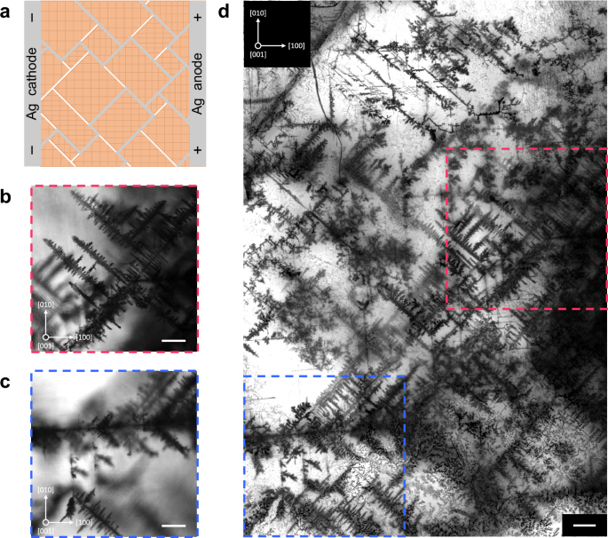
a Schematic of the experiment. The silver anode attached to the side of the sample serves as a source of silver ions. When an electric field is applied, the ions are electrophoretically injected into the crystal. The domain structure is revealed through the electrochemical reduction of silver ions to metallic silver (grey), making the domain walls (white) visible. The hatched areas represent domains with different orientations of strain. b, c Bright-field images of silver dendrites formed in MAPbBr3 monocrystal after an electric field of 24 V mm‑1 was applied for 4 h. The images show single optical slices taken at 270 µm (b) and 365 µm (c) beneath the sample surface. The scale bars are 100 µm. d Composite image with an extended depth of field, created by focus stacking 167 bright-field images. The dashed lines mark the locations where the corresponding single optical slices displayed in (b) and (c) were taken. The scale bar is 100 µm.
Fig. 2b, c show the silver-stained defect patterns in a typical solution-grown MAPbBr3 monocrystal taken near a silver electrode attached to the (100) face of the crystal (Supplementary Fig. 2a). Dendritic structures clearly indicate domain wall patterns oriented at 45° and 90° relative to the crystal axes, suggesting the presence of 90° and 180° domain walls. Domains as small as 5×5 μm2 were identified (Supplementary Fig. 2b). Fig. 2d shows an image of the silver-stained sample generated by the focal plane merging of the bright-field Z-stack, revealing a complex domain structure of the distorted cubic phase. Supplementary Movies 2 and 3 show a complete scan along the Z-axis and the reconstructed 3D structure of silver dendrites, respectively.
To evaluate the potential effects of an applied electric field (e.g., ion migration) on the intrinsic domain structure of MAPbBr3, we performed time-dependent electrochemical staining experiments (Supplementary Fig. 3, Supplementary Note 2). To that end, the electric field was applied in successive steps, and microscopic images of the sample were taken after each step. The results show that domain walls visualized at the onset of the staining process remain unchanged under repeated application of the electric field, confirming that staining reveals pre-existing domain wall patterns without altering them. We further observed that silver structures begin to disappear once the electric field is removed, which is why the microscopic images were acquired shortly after the staining process was completed. To investigate the dissolution process, we monitored the domain wall patterns in electrochemically treated samples over several days (Supplementary Fig. 4, Supplementary Note 2). During this period, the silver-stained domain walls became barely visible, indicating nearly complete dissolution of metallic silver.
Interestingly, MAPbBr3 electrophoretically doped with silver also demonstrates a reversible photochromic effect (Supplementary Fig. 5, Supplementary Note 3). This phenomenon is likely analogous to that in silver halide-containing photochromic glasses, where photochemical reduction of silver ions leads to the formation of fine metallic silver particles that strongly absorb light30.
Electrochemical staining indicates that non-cubicity in room-temperature MAPbBr3 comes in the form of microscopic ferroelastic domains each hosting different strain uniform across the domain. Importantly, in this picture strain gradients are confined to structural defects—domain walls—thus alleviating the necessity of associated stress gradients. The few-micron domain size in MAPbBr3 explains the illusion of smooth gradients of birefringence in the sample shown in Fig. 1d. The interpretation of the room-temperature phase in terms of ferroelasticity is reinforced by X-ray diffraction, which confirms the previously reported \({Pm}\bar{3}m\) space group and demonstrates the structural homogeneity of the sample (Supplementary Fig. 6, Supplementary Note 4).
Bulk photovoltaic effect
Strain gradients break inversion symmetry and generally result in electric polarization in a phenomenon known as flexoelectricity31. In light of recent reports of large voltages generated in response to externally induced mechanical deformations in MAPbBr332,33, one may wonder if spontaneous strain gradients in nominally cubic LHPs can also result in local electric polarization (Fig. 3a).
Fig. 3: Inversion symmetry breaking in MAPbBr3 evidenced by the two-photon bulk photovoltaic effect.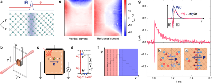
a Schematic of the strain gradient confined to the domain wall and the resulting gradients of polarization \({{{\bf{P}}}}\) and potential \(\phi\) induced by the flexoelectric effect. b Schematic of the photocurrent measurement setup. The sample can be moved relative to the beam to measure the current flowing in vertical or horizontal directions for each position of the excitation spot. c Schematic of the photoexcited carrier separation caused by internal electric fields. The dashed white line marks the part of the sample where the current measurements were performed. d Energy diagram of the two-photon absorption process. e Spatial distribution of the photocurrent measured in the vertical and horizontal directions. Each point represents the current measured when the sample is excited at the corresponding location. The scale bars are 500 µm. f Schematic of electrostatic potential distribution \(\phi (x)\) in a sample with domain-wall flexoelectricity. The dashed lines represent domain walls. g Typical time-resolved photocurrent transient acquired in a horizontal direction. The top inset illustrates the temporal evolution of polarization \({{{\bf{P}}}}\) and current \(I\) following optical excitation. The bottom inset shows schematic microscopic pictures of the charge separation and recombination phases of the photocurrent generation.
Here, we confirm the presence of local electric polarization in bulk MAPbBr3 by detecting zero-bias photocurrent in as-grown single-crystal samples following localized photocarrier injection. To this end, an ultrafast sub-bandgap laser pulse is focused inside the sample, generating electron-hole pairs deep inside the bulk through two-photon absorption34,35 (Fig. 3b–d, Supplementary Figs. 7–10, Supplementary Note 5). The photocurrent is picked up through two pairs (for vertical and horizontal currents) of non-metallic carbon leads attached to the sides of the sample by a lock-in amplifier in current detection mode (Methods). The measurements were performed on the same sample as in the birefringence measurements shown in Fig. 1d. Fig. 3e shows maps of the current frequency component corresponding to the laser pulse repetition rate (\({f}_{{{{\rm{rep}}}}}\) = 1.5 kHz) \({I}_{{{{\rm{rep}}}}}\) obtained by scanning the beam across the sample. It is evident that the current \({I}_{{{{\rm{rep}}}}}\) strongly depends on the location of carrier injection. Notably, the sign of \({I}_{{{{\rm{rep}}}}}\) remains constant across large sections of the sample, which are not symmetrical with respect to the midplane of the sample, indicating that the photocurrent is likely not due to dynamic flexoelectricity36. Instead, it can be understood in terms of electrostatic potential distribution \(\phi (x)\) in a sample with domain-wall flexoelectricity as shown schematically in Fig. 3f. Here, the plateaus represent regions of constant strain and \(\phi (x)\) within domains that both change abruptly at domain walls; the sign of photocurrent \({I}_{{{{\rm{rep}}}}}\) is then determined by the average slope of electrostatic potential.
This picture offers a natural explanation to the conflicting phenomenology of the apparent ferroelectricity in LHPs: on the one hand, flexoelectric polarization at domain walls related to the difference in structure between domains naturally explains the observed pyroelectric phenomena at structural phase transitions (e.g., ref. 16), and the pinning of domains walls can account for hysteretic polarization under external electric field14,15. On the other, flexoelectric polarization remains confined to the domain walls, keeping inversion symmetry intact in bulk, in full agreement with optical second-harmonic generation experiments37,38.
The zero-bias two-photon photocurrent was also observed in bulk MAPbI3, upon optical excitation of a single-crystal sample (Supplementary Fig. 14, Supplementary Note 7). Although the exact nature of the inversion symmetry breaking evidenced by the observation of zero-bias photocurrent cannot be established without further investigation, there are indications that it may originate from flexoelectric domain walls. MAPbI3 is tetragonal at room temperature and shows behavior sometimes interpreted as evidence of ferroelectric ordering14,15. However, ferroelectricity is inconsistent with second-harmonic generation studies37,39,40, which confirm the presence of bulk inversion symmetry. Moreover, the photovoltaic efficiency of MAPbI3 reportedly remains unaffected by the tetragonal-to-cubic phase transition25. These observations can be naturally explained by localized flexoelectricity present in both phases, suggesting that flexoelectric domain walls are not exclusive to MAPbBr3 but may constitute a unifying origin of local inversion symmetry breaking in LHPs.