
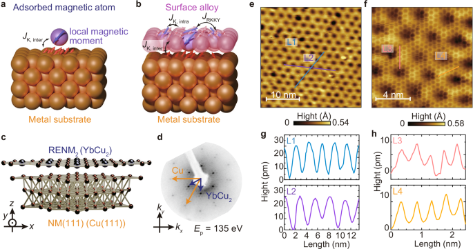
We begin by confirming the interfacial moiré atomic structure of YbCu2/Cu(111) through LEED and STM measurements. In the LEED pattern shown in Fig. 1d, clear periodic (\(\sqrt{3}\times \sqrt{3}\))R30° and primitive (1 × 1) spots originating from YbCu2 and Cu(111) are observed, as indicated by the blue and orange arrows, respectively. In addition, moiré patterns due to the lattice mismatch between YbCu2 and Cu(111) appear, similar to those reported for other RE NM2/NM(111) surfaces22,24,27,28. To further examine the real-space distribution of YbCu2/Cu(111), STM topographies acquired at 80 K are shown in Fig. 1e, f. The atomically resolved image in Fig. 1f reveals the coexistence of the atomic lattice of the YbCu2 layer and the moiré-induced long-range order. The periodic length of the moiré superstructure and the atomic distance of the monoatomic YbCu2 layer are evaluated as 25 ± 2 Å and 4.6 ± 0.2 Å, respectively, as shown in the line profiles in Fig. 1g, h. These values are reasonable with those reported for other RENM2/NM(111)24,28. The presence of a well-defined moiré pattern demonstrates the high quality of the YbCu2/Cu(111) interface used in this study. A comparison between scanning tunneling spectroscopy and ARPES is provided in Suppl. Note 1.
Figure 2a shows wide-range ARPES intensity plot of YbCu2/Cu(111) along \(\bar{\Gamma }\) – \(\bar{{{{\rm{K}}}}}\) taken with horizontally polarized 37 eV photons at 7 K. Experimental geometry for ARPES is shown in Supplementary Note 2. The Yb2+ 4f7/2 and 4f5/2 flat bands are located near the binding energies of 0 eV (EF) and 1.1 eV, originating from the Yb final state after photoexcitation. The well-dispersive hole band A, which is a lower branch of the 2D c-f hybridization band on YbCu2 around the \(\bar{\Gamma }\) point, is visible30. The outside of the higher wavenumber than that of band B has relatively strong photoelectron intensity due to a bulk band projection folded by \((\sqrt{3}\times \sqrt{3})\)R30° surface periodicity31. The details of band B will be discussed later. The shape of the electron band C is similar to that of the parabolic band on the Cu(111) clean surface, as shown in Fig. 2b. Note that band C in YbCu2/Cu(111) has almost no photoelectron intensity in the binding-energy range from EF to approximately 0.2 eV, as it is hidden in the bulk band projection.
Fig. 2: Surface electronic structures of YbCu2/Cu(111).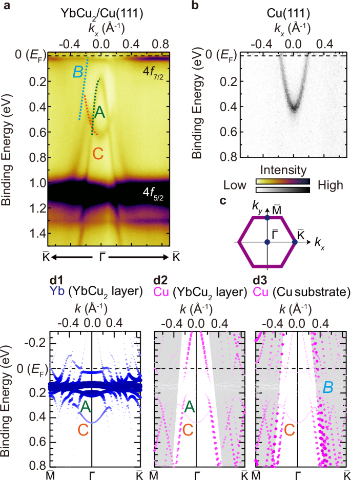
a ARPES intensity plots along \(\bar{\Gamma }\)–\(\bar{{{{\rm{K}}}}}\) taken with horizontally polarized 37 eV photons at 7 K. b same as (a) but Cu(111) clean surface. c A hexagonal surface Brillouin zone of YbCu2/Cu(111). kx and ky are defined along \(\bar{\Gamma }\)–\(\bar{{{{\rm{K}}}}}\) and \(\bar{\Gamma }\)–\(\bar{{{{\rm{M}}}}}\) of YbCu2. d1−d3 Calculated band structure of YbCu2/Cu(111), where the radii of the circles represent the projected contribution of (d1) all Yb, (d2) Cu atom in the YbCu2 layer, and (d3) Cu atom in the substrate.
Comparing experimental results with theoretical calculations is useful for identifying the origin of the observed band structure. Figure 2d presents the calculated element- and layer-resolved band dispersions of YbCu2/Cu(111). To capture the overall features of the electronic structure, a calculation without electron correlation effects is also sufficient. Theoretical band C is well reproduced in the ARPES results, exhibiting a parabolic dispersion, despite having a strong orbital contribution from Yb atoms. Notably, in calculations for free-standing YbCu2, such a parabolic band never appears in the occupied states30, indicating that the origin of band C lies in the presence of the Cu(111) substrate. In contrast, band A originates from the topmost YbCu2 layer, but band B does not appear in the topmost layer but belongs to the Cu substrate, as shown in Fig. 2d2−d3. As shown in Fig. 1c, although the YbCu2 layer and the Cu(111) substrate are spatially separated, the Yb character still contributes to band B, which may indicate an interaction between the topmost Yb atoms and the Cu(111) substrate. The possible interfacial interaction, based on the distance between YbCu2 and Cu(111), is discussed in Suppl. Note 3. It should be noted that the DFT calculations assume a substrate-matched \((\sqrt{3}\times \sqrt{3})\)R30° structure, rather than the large slab incorporating the moiré superstructure observed in LEED and STM. Consequently, band B originates from the folding of the bulk conduction band of the Cu substrate by the \((\sqrt{3}\times \sqrt{3})\)R30° periodicity, independent of the moiré superstructure.
The interfacial interaction between the YbCu2 layer and Cu(111) would satisfy the condition for the formation of interfacial HF via the interfacial exchange coupling JK,inter, as illustrated in Fig. 1(b). Evidence for interfacial HF should appear at the crossing point between the Yb 4f state near EF and the bulk-derived hole band B. Figure 3a presents a high-resolution ARPES image of YbCu2/Cu(111) near EF, obtained with horizontally polarized 33-eV photons at 7 K. To visualize the band structure above EF, the ARPES intensities were divided by the Fermi-Dirac distribution function convolved with the instrumental resolution. Several hole bands clearly cross EF around the \(\bar{\Gamma }\) point. The asymmetric photoelectron intensity of the Yb2+ 4f7/2 states can be attributed to photoexcitation selection rules. To clarify the conduction bands, the momentum-distribution curve (MDC) at EF, corresponding to the cross-section of the Fermi surface, is shown in Fig. 3b. In addition to the steep band Aupper, which is the upper branch of the 2DHF state on the YbCu2 layer30, another hole band, Bupper, with a Fermi wavenumber kF of 0.2 Å−1 is observed at EF. The broad intensity tail toward higher momentum on the positive wavenumber side is likely due to kz broadening induced by vacuum-ultraviolet photoexcitation. Figure 3c shows the energy distribution curves from Fig. 3a at 0.0 Å−1 (\(\bar{\Gamma }\) point) and 0.4 Å−1. The energy position of the Yb2+ 4f7/2 states is slightly shifted by approximately 10 meV near the crossing point with hole band B, which lies at the boundary of the bulk band projection discussed above. Such a momentum-dependent energy shift of the Yb2+ 4f state never appears in disordered cases, such as the single-atom adsorption case or randomly diffused Yb atoms in the Cu(111) substrate, indicating coherent Kondo effect JK,inter as illustrated in Fig. 1b. Moreover, the left branch of band B smoothly connects to the Yb2+ 4f7/2 state, providing direct evidence of hybridization between the Yb 4f state and band B.
Fig. 3: Interfacial c-f hybridization in YbCu2/Cu(111).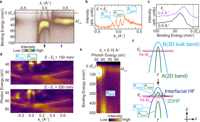
a High-resolution ARPES image near the \(\bar{\Gamma }\) point taken with horizontally polarized 33 eV photons at 7 K. ARPES intensities are divided by the Fermi–Dirac distribution function convolved with the instrumental resolution. b Momentum distribution curves at EF taken from (a) with the energy windows of ± 10 meV. c Energy distribution curves (EDCs) at kx = 0.0 and 0.4 Å−1. The kx positions are indicated by arrows in (a). d Photon-energy dependence of MDCs at the normal emission at binding energies of 150 meV (upper panel) and 250 meV (lower panel) with the energy windows of ± 10 meV. e Photon-energy dependence of EDCs at kx = 0.15 Å−1. The dashed lines are drawn as guides to the eye. f The schematics of HF formation of YbCu2/Cu(111) around \(\bar{\Gamma }\) point.
To obtain further information on hybridization, the photon-energy dependence of the YbCu2 layer at binding energies of 150 meV and 250 meV, was measured as shown in Fig. 3d. As noted in Fig. 3a, the lower branches of bands A and B exhibit stronger photoelectron intensities than their upper branches. The outer dispersion, indicated by yellow curves, originates from the Cu bulk sp bands. Band A shows no photon-energy dependence, whereas band B clearly exhibits obvious photon-energy dependence, indicating that band B possesses a 3D character. Figure 3e shows the photon-energy dependence of the EDCs at kx = 0.15 Å−1. The raw data of the photon-energy-dependent ARPES measurements are provided in Supplementary Note 4. The band B shows a clear dispersion along kz. In particular, the strong photoemission intensity was observed around hν = 35 eV, suggesting the presence of a crossing point between 3D hole band and Yb2+ 4f7/2 along the out-of-plane direction.
These results strongly suggest that the bulk conduction band derived from Cu(111) and the Yb 4f states in the surface YbCu2 layer establish an interfacial hybridization band at the YbCu2/Cu(111) interface. Figure 3g presents a schematic illustration of HF formation in YbCu2/Cu(111). At the \(\bar{\Gamma }\) point, two types of hole bands and the Yb 4f states are located. As indicated by the DFT calculations, the innermost hole band appears to originate from the YbCu2 surface layer, whereas the outer hole band is derived from the Cu(111) substrate. Through c-f hybridization, these hole bands interact with the Yb 4f states, leading to the formation of both a 2DHF and an interfacial 3DHF state. It should be noted that the moiré superlattice, due to slight twist angles, is not necessarily required for the development of interfacial HF. Instead, it is the flat band generated by the long-period potential, which corresponds to localized electrons, that contributes to interfacial HF formation through interfacial exchange interactions.
In HF systems, the size of the Fermi surface corresponding to kF, expands below the single-site Kondo temperature due to the development of c-f hybridization32,33. Figure 4a shows the temperature-dependent ARPES intensity plots of YbCu2/Cu(111) along \(\bar{\Gamma }\)-\(\bar{{{{\rm{K}}}}}\), measured with horizontally polarized 33 eV photons. The raw data of the temperature-dependent ARPES measurements are provided in Suppl. Note 5. At first glance, the band dispersion near EF exhibits slight temperature-dependent modulations. To gain deeper insight into the temperature evolution of the kF, MDCs at EB = 0 eV are shown in Fig. 4b. Two pairs of peaks were identified: C1, derived from Aupper, and C2, derived from Bupper. As the temperature decreases, the kF of C1 expands, while that of C2 remains nearly unchanged. Figure 4c1, c2 display the averaged peak positions of C1 and C2, respectively, obtained by fitting the MDC curves in Fig. 4b with Lorentzian functions. The kF of C1 monotonically increases with decreasing temperature, and this trend continues across the coherence temperature (Tcoh) of the monoatomic-layer YbCu2. A slight change in the rate of increase is observed around 30 K, consistent with the temperature dependence of the Kondo resonance peak30.
Fig. 4: Temperature dependence of interfacial c-f hybridization in YbCu2/Cu(111).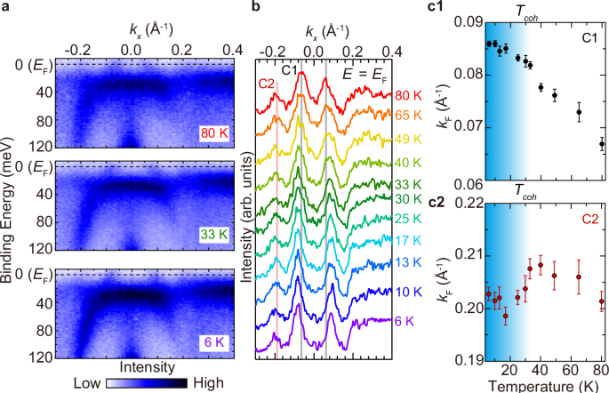
a Temperature-dependent ARPES image near the \(\bar{\Gamma }\) point taken with horizontally polarized 33-eV photons. ARPES intensities are divided by the Fermi–Dirac distribution function convolved with the instrumental resolution. b MDCs at EF as a function of the temperature. c1 Momentum dependence of the kF of S1 plotted on a linear scale of temperature. c2 Same as (c1) but for S2. The shaded area indicates the coherent temperature Tcoh of the 2DHF state of monoatimic-layer YbCu2. Error bars are determined by the standard deviation of the fits to the data.
In contrast, the variation in the kF of C2 is relatively weak compared with that of C1, indicating that the temperature-dependent renormalization is weaker, implying that the Kondo temperature of the interfacial HF in YbCu2/Cu(111) differs from that of the 2DHF state in the monoatomic-layer YbCu2.
We have revealed that the interfacial HF coexists with the 2DHF in YbCu2/Cu(111). Note that the hybridization partners of the conduction electrons for both the 2D HF and the interfacial HF are the 4f states of the same Yb atoms, which occupy a single crystallographic site in the YbCu2 layer, as shown in the STM images in Fig. 1f, g. The 2DHF state is expected to couple predominantly with in-plane orbitals owing to the monoatomic-layer geometry, whereas the interfacial coupling should occur along the out-of-plane direction. The orbital symmetry of Yb 4f states probed by polarization-dependent ARPES is shown in Suppl. Note 6. This implies that the origin of the interfacial HF, as well as its coexistence with the 2DHF in YbCu2/Cu(111), arises from orbital-selective c-f hybridization. Furthermore, the fact that different orbitals at a single site hybridize may account for the changes observed below the Tcoh of the 2DHF. The presence of two hybridization channels in a Kondo lattice could, as in the case of the anomalous Seebeck coefficient reported for twisted bilayer graphene34, provide a possible origin for the emergence of novel and unconventional quantum phenomena.
Interestingly, STM images clearly reveal periodic modulations in the topography consistent with the moiré periodicity, suggesting that the moiré potential could locally modulate the HF state. The possible influence of the moiré structure of YbCu2 on HF formation is discussed in Suppl. Note 7. Future investigations, such as low-temperature scanning tunneling spectroscopy (STS) with atomic-scale spatial resolution, will be crucial for elucidating how the moiré potential affects the formation and local modulation of the HF state.