
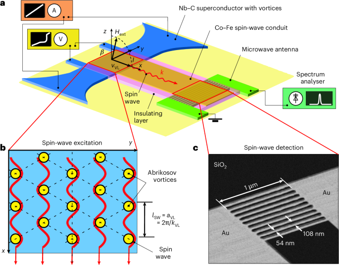
Fabrication of the microwave nano-antenna
The fabrication of the experimental system began with the deposition of a 40/5 nm Au/Cr film onto a Si (100 nm, p-doped)/SiO2 (200 nm) substrate and its patterning for electrical d.c. current and microwave measurements. In the sputtering process, the substrate temperature was 22 °C, the growth rates were 0.055 nm s−1 and 0.25 nm s−1, and the Ar pressures were 2 × 10⁻³ mbar and 7 × 10⁻³ mbar for the Cr and Au layers, respectively. The microwave ladder antenna was fabricated from the Au/Cr film by focused ion beam milling at 30 kV/30 pA in a dual-beam scanning electron microscope (FEI Nova Nanolab 600). The multi-element antenna consisted of ten nanowires connected in parallel between the signal and ground leads of a 50-Ω-matched microwave transmission line. The antenna had a period p = 108 nm with the nanowire width equal to the nanowire spacing so that its Fourier transform contained only odd spatial harmonics with\({\lambda}_{1}=p\) and \({\lambda}_{3}=p/3=36\,{\rm{nm}}\), which made it sensitive to spin-wave wavelengths of 36 ± 2 nm in our experiments (Supplementary Fig. 1).
Fabrication and properties of the Nb–C microstrip
The ladder antenna’s fabrication was followed by direct writing of the superconducting strip at 2 μm (edge to edge) from the microwave antenna. The 45-nm-thick Nb–C microstrip was fabricated by focused ion beam-induced deposition. Focused ion beam-induced deposition was done at 30 kV/10 pA, 30 nm pitch and 200 ns dwell time employing Nb(NMe2)3(N-t-Bu) as precursor gas26. The superconducting strip and the ladder antenna were covered with a 3-nm-thick insulating Nb–C layer prepared by focused electron beam-induced deposition (FEBID). Before the Co–Fe magnonic waveguide deposition, a 48-nm-thick insulating Nb–C–FEBID layer was deposited to compensate for the structure height variations between the antenna and the Nb–C strip. The elemental composition in the Nb–C strip was 45 ± 2 at.% C, 29 ± 2 at.% Nb, 15 ± 2 at.% Ga and 13 ± 2 at.% N, as inferred from energy-dispersive X-ray spectroscopy on thicker microstrips written with the same deposition parameters. The Nb–C strip had well-defined smooth edges and a root mean squared surface roughness of <0.3 nm, as deduced from atomic force microscopy scans over its 1 μm × 1 μm active part before the deposition of the Co–Fe layer. The two ends of the strip had rounded sections to prevent current crowding effects at the sharp strip edges, which may lead to an undesirable reduction of the experimentally measured critical current and the instability current45.
The resistivity of the Nb–C microstrip at 7 K was \(\rho_{7{\rm{K}}}=551\,\upmu{\Omega}\,{\rm{cm}}\). The microstrip transitioned to a superconducting state below the transition temperature Tc = 5.60 K, deduced using a 50% resistance drop criterion. Application of a magnetic field Hext ≈ 2 T led to a decrease of Tc(0) to Tc(2 T) ≈ 5.1 K. Near Tc, the critical field slope \((\mathrm{d}{H}_{{\rm{c2}}}/\mathrm{d}T){| }_{{T}_{{\rm{c}}}}=-2.19\) T K−1 corresponds, in the dirty superconductor, to the electron diffusivity \(D=-4{k}_\mathrm{B}/(\pi e(\mathrm{d}{H}_{{\rm{c2}}}/\mathrm{d}T){| }_{{T}_{{\rm{c}}}})\approx 0.5\) cm2 s−1 with the extrapolated zero-temperature upper critical field value Hc2(0) ≈ 12.3 T. Here, kB is the Boltzmann constant and e the elementary charge. The coherence length and the penetration depth at zero temperature were estimated46 as \({\xi }_{\mathrm{c}}={(\hslash D/{k}_{\mathrm{B}}{T}_{\mathrm{c}})}^{1/2}\approx 9\,{\mathrm{nm}}\) (corresponding to \({\xi}(0)={\xi}_{\rm{c}}{(1.76)}^{-1/2}\approx7\,{\rm{nm}}\)) and \(\lambda (0)=1.05\times 1{0}^{-3}{({\rho }_{{\rm{7K}}}{k}_\mathrm{B}/\varDelta (0))}^{1/2}\approx \text{1,040}\,{\mathrm{nm}}\). Here, \({\varDelta}(0)\) is the zero-temperature superconducting energy gap and \(\hslash\) is the Planck constant.
Fabrication and properties of the Co–Fe conduit
The Co–Fe magnonic conduit was 1μm wide, 5 μm long and 30 nm thick. We fabricated it by FEBID employing HCo3Fe(CO)12 as the precursor gas47. FEBID was done with 5 kV/1.6 nA, 20 nm pitch and 1 μs dwell time. The material composition in the magnonic waveguide is 61 ± 3 at.% Co, 20 ± 3 at.% Fe, 11 ± 3 at.% C and 8 ± 3 at.% C. The oxygen and carbon are residues from the precursor in the FEBID process47. The Co–Fe conduit consisted of a dominating bcc Co3Fe phase mixed with a minor amount of FeCo2O4 spinel oxide phase with nanograins of about 5 nm in diameter. The random orientation of Co–Fe grains in the carbonaceous matrix ensured negligible magnetocrystalline anisotropy. Further details on the microstructural and magneto-transport properties of Co–Fe–FEBID were reported previously47.
Electrical resistance measurements
The I–V curves were recorded in current-driven mode within a 4He cryostat fitted with a superconducting solenoid. The external magnetic field Hext was tilted at a small angle \(\beta={5}^{\circ}\) with respect to the normal to the sample plane (z axis) in the plane perpendicular to the direction of the transport current. The small field tilt angle \(\beta\) ensures that the field component Hext,z acting along the z axis is only negligibly smaller than Hext with (Hext − Hext,z)/Hext ≤ 0.5%. The transport current applied along the y axis in a magnetic field H ≈ Hext = Hz exerts on vortices a Lorentz force acting along the x axis28. The voltage induced by the vortex motion across the superconducting microstrip was measured with a nanovoltmeter. A series of reference measurements was taken before the deposition of the Co–Fe magnonic conduit on top of the Nb–C strip. No voltage steps were revealed in the I–V curves of the bare Nb–C strip. By contrast, constant-voltage steps in the I–V curves were revealed after the deposition of the Co–Fe magnonic conduit on top of the Nb–C strip. The rarely achieved combination of weak volume pinning, in conjunction with close-to-perfect edge barriers and a fast relaxation of nonequilibrium electrons, allows for ultrafast motion of Abrikosov vortices in the Nb–C superconductor31.
Microwave detection of spin waves
The microwave detection of spin waves was performed using a microwave ladder nano-antenna connected to a spectrometer system. This allowed detecting signals at power levels down to 10−16 W in a 25 MHz bandwidth32. The detector system consisted of a spectrum analyser (Keysight Technologies N9020B, 10–50 GHz), a semirigid coaxial cable (SS304/BeCu, d.c.–61 GHz) and an ultrawide-band low-noise amplifier (RF-Lambda RLNA00M54GA, 0.05–54 GHz, +20 dB gain).
Micromagnetic simulations
The micromagnetic simulations were performed using the graphics processing unit-accelerated simulation package MuMax3 to calculate the investigated structures’ space- and time-dependent magnetization dynamics41. The simulations were done for the following Co–Fe parameters: saturation magnetization Ms = 1.4–1.5 MA m−1, exchange constant A = 15–18 pJ m−1 and Gilbert damping \({\alpha}=0.01\). The best match of the simulation results with the experimental data has been revealed for Ms = 1.45 MA m−1 and A = 15 pJ m−1. The mesh was set to 2 × 2 nm2, which is smaller than the exchange length of Co–Fe (~5 nm) and fulfils the requirements for micromagnetic simulations. The simulations were validated by comparing with the results obtained within the Kalinikos–Slavin theory48 (Supplementary Fig. 3). The estimated attenuation length of the generated magnons (at kSW ≈ 175 rad μm−1) is around 600 nm (ref. 48).
An external field Hext in the range 1.75–1.95 T, sufficient to magnetize the structure to saturation, was applied at a small angle \(\beta\) relative to the z axis in the x–z plane (Supplementary Fig. 4). A fast-moving periodic field modulation was used to mimic the effect of the moving vortex lattice. The oscillations mx(x, y, t) were calculated for all cells and all times via mx(x, y, t) = Mx(x, y, t) − Mx(x, y, 0), where Mx(x, y, 0) corresponds to the ground state (fully relaxed state without any moving magnetic field source). The dispersion curves were obtained by performing two-dimensional fast Fourier transformations of the time- and space-dependent data. The spin-wave spectra were calculated by performing a fast Fourier transformation of the data in a region at a distance of 1 μm from the spin-wave excitation region (Supplementary Fig. 5). Full details on the micromagnetic simulations are given in Supplementary Note 1. The evolution of the magnon generation condition upon variation of the magnetization, exchange stiffness and thickness of the Co–Fe conduit is illustrated in Supplementary Figs. 6–9. The observed magnon generation may be interpreted by two scenarios, namely the coherent fluxon-magnon coupling and the magnonic Cherenkov effect. The relation between the Cherenkov effect for single and multiple periodically arranged moving particles is illustrated in Supplementary Fig. 10.
Ginzburg–Landau simulations
The evolution of the superconducting order parameter \({\varDelta}=|{\varDelta}|{e}^{i{\varPhi}}\) was analysed relying upon a numerical solution of the modified TDGL equation49, solved in conjunction with the heat-balance equation, to account for possible heating effects
$$\begin{array}{r}\displaystyle\frac{\pi \hslash }{8{k}_{{\rm{B}}}{T}_{{\rm{c}}}}\left(\displaystyle\frac{\partial }{\partial t}+\frac{2ie\varphi }{\hslash }\right)\varDelta =\\ ={\xi }_{{\rm{mod}}}^{2}{\left(\nabla -i\displaystyle\frac{2e}{\hslash c}\mathbf{A}\right)}^{2}\varDelta +\left(1-\displaystyle\frac{{T}_{{\rm{e}}}}{{T}_{{\rm{c}}}}-\displaystyle\frac{| \varDelta {| }^{2}}{{\Delta }_\mathrm{mod}^{2}}\right)\varDelta +\\ +i\displaystyle\frac{({\rm{div}}\,{{\bf{j}}}_{{\rm{s}}}^{{\rm{Us}}}-{\rm{div}}\,{{\bf{j}}}_{{\rm{s}}}^{{\rm{GL}}})}{| \varDelta {| }^{2}}\frac{e\varDelta \hslash D}{{\sigma }_{{\rm{n}}}\sqrt{2}\sqrt{1+{T}_{{\rm{e}}}/{T}_{{\rm{c}}}}},\end{array}$$
where \({\xi }_{{\rm{mod}}}^{2}=\pi \sqrt{2}\hslash D/(8{k}_{{\rm{B}}}{T}_{{\rm{c}}}\sqrt{1+{T}_{{\rm{e}}}/{T}_{{\rm{c}}}})\), \({\varDelta }_{{\rm{mod}}}^{2}={({\varDelta }_{0}\tanh (1.74\sqrt{{T}_{{\rm{c}}}/{T}_{{\rm{e}}}-1}))}^{2}\)\(/(1-{T}_{{\rm{e}}}/{T}_{{\rm{c}}})\), A is the vector potential, φ is the electrostatic potential, D is the diffusion coefficient, \({\sigma}_{\rm{n}}=2{e}^{2}DN(0)\) is the normal-state conductivity with N(0) being the single-spin density of states at the Fermi level, Te and Tp are the electron and phonon temperatures, and \({{\bf{j}}}_{{\rm{s}}}^{{\rm{Us}}}\) and \({{\bf{j}}}_{s}^{{\rm{GL}}}\) are the superconducting current densities in the Usadel and Ginzburg–Landau models
$${{\bf{j}}}_{{\rm{s}}}^{{\rm{Us}}}=\frac{\pi {\sigma }_{{\rm{n}}}}{2e\hslash }| \varDelta | \tanh \left(\frac{| \varDelta | }{2{k}_{{\rm{B}}}{T}_{{\rm{e}}}}\right){{\bf{q}}}_{{\rm{s}}},$$
(1)
where \({\bf{q}}_{\rm{s}}={\nabla}{\varphi}+2{\pi}{\bf{A}}/{\varPhi}_{0}\) and \({{\bf{j}}}_{{\rm{s}}}^{{\rm{GL}}}=\frac{\pi {\sigma }_{{\rm{n}}}| \varDelta {| }^{2}}{4e{k}_{{\rm{B}}}{T}_{{\rm{c}}}\hslash }{{\bf{q}}}_{{\rm{s}}}\).
The vector potential A = (0, Ay, 0) in the TDGL equation consists of two parts: Ay = Hextx + Am, where Hext is the external magnetic field and Am is the vector potential of the magnetic field induced in the superconducting strip by spin waves.
The modelled length of the microstrip is L = 4w, the width \(w=50{\xi}_{c}\), and the parameter \({B}_{0}={\varPhi}_{0}/(2{{\pi}}{\xi}_{\rm{c}}^{2})\approx 4.15\,{\rm{T}}\), where \({\xi}_{c}=8.9\,{\rm{nm}}\). The calculations were done with parameters \(\gamma=9\) and \({\tau}_{0}=925\,{\rm{ns}}\) for NbN, as their values for NbC are unknown but are supposed to be of the same order of magnitude. A variation of \(\gamma\) and \(\tau\) only leads to quantitative changes in the I–V curves and does not qualitatively change the vortex dynamics. In simulations, dA was varied between 0 (no ferromagnet layer) and \(0.1{\varPhi}_{0}/(2{\pi}{\xi}_{\rm{c}})\), which corresponds to about 1/4 of the depairing velocity for superconducting charge carriers (Cooper pairs) or critical \(q_{\rm{sc}}0.35\,{\varPhi}_{0}/2{\pi}{\xi}_{\rm{c}}\) of the superconducting strip at B = 0 and T = 0.8Tc. The parameters ax and ay were chosen to model a triangular moving vortex lattice without the ferromagnetic layer and far from the instability point. We present the results for \({v}=110{\xi}_{\rm{c}}/{\tau}_{0},\,{a}_{x}=5.5{\xi}_{\rm{c}}\) and \({a}_{y}=9.2{\xi}_{\rm{c}}(a_{\rm{VL}}=4.9{\xi}_{\rm{c}}\,{\rm{at}}\, B=0.3\,B_{0})\). We find that the width and the slope of the plateau in the I–V curve weakly vary with small variations of ax and ay, while the value of vm controls the voltage plateau position.
Further details on the TDGL simulations are given in Supplementary Note 2. The TDGL modelling results are presented in Extended Data Fig. 1. The animated spatiotemporal evolutions of the superconducting order parameter are shown in Supplementary Videos 4–12.