
Sample preparation
Our WSe2 samples are grown via metal organic chemical vapor deposition on few-layer epitaxial graphene supported by a conductive silicon carbide (c-SiC) substrate. The plasma frequency of c-SiC is sufficient to effectively suppress THz reflections from the bottom surface. Intercalation of the graphene layers with hydrogen prior to WSe2 growth terminates the dangling silicon bonds, providing a homogeneous electrostatic background. Further details of the sample growth procedure were previously reported along references16,43. Key advantages of epitaxially grown samples on quasi-free-standing graphene (QFEG) are the electronic homogeneity (no moiré), a Fermi energy pinned in the center of the large WSe2 band gap, and weak hybridization with the substrate16. The strong out-of-plane confinement facilitates electron-phonon coupling, well-defined defect states, and high contrast of the defect states inside the band gap, enabling LW-STM at nonzero Vdc.
High-temperature annealing in UHV is required to clean samples after ambient exposure. We generate isolated VacSe in the top WSe2 layer via light sputtering with Ar ions, approximately 2 s at 0.12 kV acceleration bias, 0.16 kV discharge voltage, and a sub-μA sputter-current16. Multiple VacSe in 1–2 ML WSe2 were investigated for this study, emphasizing the robustness and repeatability of the technique. Fig. S1 lists STM topography, dI/dV spectra, and current saturation curves of the relevant VacSe.
STM height set point and average charge-state lifetime
For a reproducible definition of the tip height z0, the STM feedback loop was opened on pristine WSe2 at a set point current of 100 pA with applied bias voltage of 1.5 V (1 ML) or 1.2 V (2 ML), corresponding to an energy 200 meV above the conduction band onset. We estimate an absolute tip–sample distance at z0 of (7 ± 2) Å. The average charge-state lifetime (τ0) of VacSe states scales with the decoupling layers of the sample and is determined via the current saturation in STM approach curves15,16,32. For simplicity, we consider only the first unoccupied defect state (LUMO) of VacSe for the determination of τ0. Reduced localization due to a lower binding energy slightly reduces the average charge-state lifetime of the LUMO+1 defect state16. For different VacSe, τ0 slightly vary due to differences in their dielectric environment, however, the energy spectra and orbital shape remain comparable within a few-10 meV shifts (Fig. S1).
Voltage drop and definition of ΔV
In our double barrier tunneling junction geometry, the effective voltage from the tip to the VacSe defect states depends on the WSe2 dielectric screening and the absolute height set point z0. The relative voltage ΔV = Vdc − VLUMO(z) is important to compare LW-STM data across different VacSe, where the onset of the LUMO, VLUMO(z), varies on the order of tens of meV due to inhomogeneity of the sample and as a function of z. While for ΔV < 0 the dc current is negligible, ΔV > 0 V generates a notable dc current and thus increases the VacSe population statically in the experiment. In orbital imaging, we define ΔV at a single point on the orbital lobe of VacSe, avoiding complications of lateral dependence. We determine VLUMO(z) directly from a dI/dV measurement at z or via extrapolation of VLUMO(z0) on the basis of measurements performed in ref. 16, Fig. 2. Owing to the high sensitivity towards thermal drifts on the sub-Å scale, we estimate an accuracy δΔV ≈ 10 mV.
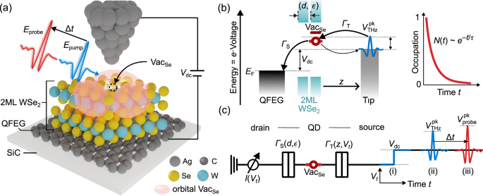
LW-STM setup and near-field waveform detection
Our LW-STM system is a commercial low-temperature STM from CreaTec Fischer & Co. GmbH with free-space optical access to the STM junction via large numerical aperture parabolic mirrors focused on the tip apex. THz pulses are generated via tilted pulse front optical rectification in lithium niobate pumped by a multi-MHz Yb:fiber laser with pump pulse energies of a few μJ. The system achieves peak THz voltages at the STM tip up to 0.5, 1, and 2 V at 41, 20, and 10 MHz repetition rates, respectively. We use frustrated internal reflection in a PTFE prism as well as a double or single mirror sequence to adapt the phase and polarity of single-cycle THz pulses at the STM tip44. Pump and probe pulses are generated independently and are recombined in collinear geometry via a c-cut sapphire window. Purging of the optics setup with dry air reduces ambient absorption before pulses are coupled into the vacuum chamber. Operating conditions of the scanning probe microscope are 5 K base temperature and 10−10 mbar pressure.
To discriminate lightwave-driven currents, we mechanically modulate the THz path at an intermediate focus using frequencies between 800 and 1000 Hz that are compatible with the 109 transimpedance amplifier of the STM and show weak mechanical and electric noise. ILW is then extracted via lock-in demodulation and calibrated with respect to the absolute current. We convert current to rectified charge per transient (e/tr) on the basis of the laser repetition rate and the 50% duty cycle of the modulation. In pump-probe measurements, only the probe pulse is modulated, while pump pulses enter the junction at full repetition rate. We find that high DC currents prevent sensitive measurements of QLW because of large noise floors.
The THz peak voltage is calibrated against Vdc using a recently developed approach based on the strongly nonlinear onset of the WSe2 conduction band31 measured in a clean pristine region of the sample (Fig. S2a–c). On the basis of this amplitude calibration, we determine the relative time origin (Δt = 0) and temporal resolution of the experiment (380 fs) by cross correlation of equal THz fields where only the sum field rectifies charges (Fig. S2d). In a second step, we measure the transient near-field waveform at the STM tip using THz cross correlation (THz-CC)29,31. Here, we set relative amplitudes such that a strong THz gate pulse rectifies electrons to the conduction band in a linear section of the dI/dV curve, while a time-delayed weak THz pulse modulates the THz peak voltage. This approach allows waveform characterization without requiring complex retrieval algorithms31,45 (Fig. S2e, f). Waveform sampling at extended delays reveals THz reflections at approximately 40, 60, 80, 100, and 120 ps due to sapphire windows of the vacuum chamber, cryostat, and the beam combiner, which are unavoidable in our setup (Fig. S2g). Thickness variation of sapphire windows and the beam combiner effectively reduces the amplitude of major THz reflection to below 30% of the main pulse, causing reflections at 40 and 80 ps to show distorted waveforms due to interference effects.
Theoretical model
The dynamics observed in the tunnel junction can be well represented by a time-dependent Markov process, which is described by the so called Master equation \(\dot{N}=M\cdot N\), where N is a vector containing the occupation probabilities of all considered states of the system and M is the transition matrix. Here, we considered three distinct electronic states: The electronic ground state at energy E0 = 0 eV, where the defect is charge neutral (Q0 = 0 e), as well as two negatively charged states (Q1,2 = −e), with an additional electron in either the LUMO (E1) or the LUMO+1 (E2). In addition, we model each electronic state with a single vibronic mode with 6 (14) vibrational excitation levels plus the vibrational ground state, yielding a total of 21 (45) different vibronic states for 2 ML (1 ML) WSe2. The different number of required vibrational levels is due to different Huang-Rhys factors between 1 ML and 2 ML WSe2 (see below).
Transition between these states can occur due to inelastic charge transfer between defect and tip or sample, or via vibrational relaxation within one electronic state. Accordingly, the transition matrix can be written as the sum of the transition rates due to sample, tip and phonon relaxation:
$$M={M}^{{{{\rm{s}}}}}+{M}^{{{{\rm{t}}}}}+{M}^{{{{\rm{ph}}}}}$$
(1)
The transitions related to a change of charge state are given by
$${M}_{f{\lambda }^{{\prime} }i\lambda }^{{{{\rm{s}}}}}={T}_{f{\lambda }^{{\prime} }i\lambda }({z}_{s},0)\cdot {V}_{{\lambda }^{{\prime} }\lambda }\cdot {\Upsilon }_{fi}$$
(2)
$${M}_{f{\lambda }^{{\prime} }i\lambda }^{{{{\rm{t}}}}}={T}_{f{\lambda }^{{\prime} }i\lambda }({z}_{t},V)\cdot {V}_{{\lambda }^{{\prime} }\lambda }\cdot {\Upsilon }_{fi}\cdot {\Lambda }_{fi},$$
(3)
with indices i and f representing the initial and final electronic state, λ and \({\lambda }^{{\prime} }\) the initial and final vibrational state, \({V}_{{\lambda }^{{\prime} }\lambda }\) the Franck–Condon factors, and \({T}_{f{\lambda }^{{\prime} }i\lambda }\) the tunneling matrix element, respectively. ϒfi captures the effect of various multiplicities of the involved states, and Λfi represents their relative coupling strength to the tip.
The tunneling matrix element \({T}_{f{\lambda }^{{\prime} }i\lambda }(z,V)\) describes the tunneling probability of an electron between the tip or sample and the defect state, depending on bias voltage V and distance z between the defect and lead:
$${T}_{f{\lambda }^{{\prime} }i\lambda }(z,V)=\left\{\begin{array}{ll} \int_{-\infty }^{V}{{{\rm{d}}}}E\,g(E-\Delta {E}_{f{\lambda }^{{\prime} }i\lambda })\,{e}^{-2\kappa z}\quad &,{{{\rm{if}}}}{Q}_{f}-{Q}_{i}=-e\\ \int_{V}^{\infty }{{{\rm{d}}}}E\,g(E+\Delta {E}_{f{\lambda }^{{\prime} }i\lambda })\,{e}^{-2\kappa z}\quad \;\;\; &,{{{\rm{if}}}}{Q}_{f}-{Q}_{i}=+ e\\ 0\, \qquad \qquad\qquad\qquad\quad\qquad\quad &,\; {{{\rm{otherwise}}}} \;\;\quad \end{array}\right.$$
(4)
with \(\Delta {E}_{f{\lambda }^{{\prime} }i\lambda }\) being the energy difference between the initial and final vibronic state and decay rate \(\kappa=\sqrt{2{m}_{e}(\phi -E+eV/2)}/\hslash\). The transition threshold is broadened by a Gaussian line shape g(E) and normalized to integrate to the quantum of conductance G0 = 2e/ℏ for z = 0.
For the Franck–Condon factors \({V}_{{\lambda }^{{\prime} }\lambda }\), we assume only a rigid shift in normal mode coordinates and negligible Duschinsky rotation46:
$${V}_{{\lambda }^{{\prime} }\lambda }=\frac{\min ({\lambda }^{{\prime} },\lambda )!}{\max ({\lambda }^{{\prime} },\lambda )!}\,{S}^{| {\lambda }^{{\prime} }-\lambda | }\,{e}^{-S}\,{\left[{L}_{\min ({\lambda }^{{\prime} },\lambda )}^{| {\lambda }^{{\prime} }-\lambda | }(S)\right]}^{2},$$
(5)
with Huang-Rhys factor S and Laguerre polynomials \({L}_{n}^{\alpha }\).
The effect of the various multiplicities on the transition rates is captured by the factor ϒfi. Since we are only considering transitions for which either the final or initial state is a singlet, we can write ϒfi = mf, with mf being the multiplicity of the final state.
The last term Λfi for the tip-mediated transitions captures the relative coupling of LUMO and LUMO+1 to the tip, which can vary with lateral tip position. The additional factor Λfi is normalized to 1 for the tip–LUMO coupling and has typical values between 0.5 and 1.0 for the tip–LUMO+1 coupling, chosen to match the experimental dI/dV spectra.
For the charge-neutral phonon relaxations, the transition matrix is written as a decay to the vibrational ground state with lifetime τph:
$${M}_{f{\lambda }^{{\prime} }i\lambda }^{{{{\rm{ph}}}}}=\left\{\begin{array}{ll}1/{\tau }_{{{{\rm{ph}}}}}\quad &{{{\rm{,\; if}}}}f=i,{\lambda }^{{\prime} }=0{{{\rm{and}}}}\lambda > 0\\ 0 \qquad\quad &,{{{\rm{otherwise.}}}} \qquad\qquad\;\;\end{array}\right.$$
(6)
Lastly, the diagonal entries of the total transition matrix are set to Mll = −∑k≠lMkl.
For static bias voltages, the master equation is solved for \(\dot{N}=0\) to obtain the bias and z dependent equilibrium occupation Neq. The dc current is then given by the net charge transfer between defect and sample \({I}_{{{{\rm{dc}}}}}={\sum }_{k}{\left({W}^{s}N\right)}_{k}\), with \({W}_{f{\lambda }^{{\prime} }i\lambda }^{s}={M}_{f{\lambda }^{{\prime} }i\lambda }^{s}\cdot ({Q}_{f}-{Q}_{i})\). In order to evaluate the evolution of the system under a transient bias voltage, the master equation is solved in discrete time steps \({N}_{i+1}-{N}_{i}=M\left(V({t}_{i})\right)\Delta t\cdot {N}_{i}\), starting from the equilibrium occupation at Vdc.
Implementation of simulation
The simulations are based on the master equation and require experimental parameters that can be obtained from static measurements of the VacSe (Fig. S1). We extracted the energies of localized defect states E1 and E2 via the zero-phonon lines and the tip coupling factor Lf,i from the experimental dI/dV spectrum at the set point z0. The average charge-state lifetime τ0, and the tunneling barrier κ were obtained via a rate equation fit to the I(z) approach curve16.
The vibronic broadening of the defect state resonances was approximated by a single vibrational mode with ℏΩ = 8 meV and a Huang-Rhys factor of S = 2.2 (2 ML) for both charge states. We find that a Gaussian lineshape with 3 meV bandwidth provides a good match with the experimental dI/dV (Fig. S6b), while being consistent with literature on VacS in WS2, observing a dominant phonon mode of 12 meV and a Huang-Rhys factor of 1.218. Considering an average 40% softening of the phonon modes in WSe2 as compared to WS247, we choose a phonon mode of ℏΩ = 8 meV, and fit the Huang-Rhys factor to the STS spectrum. For the simulations on 1 ML WSe2 we cannot directly fit the vibronic satellite peaks of the LUMO resonance. Instead, we rescale the Huang-Rhys factor from 2 ML WSe2 by a factor of about two, as previously found for CS in 1 ML and 2 ML WS219. Therefore, we choose S = 5 for VacSe in 1 ML WSe2, while we assume the phonon mode energy to remain constant, ℏΩ = 8 meV19.
Although lifetime broadening of a state with tens of picoseconds of lifetime would lead to a Lorentzian lineshape with a few tens of μeV broadening, we justify the choice of Gaussian lineshapes by the presence of additional low-energy vibrational modes with a high Huang-Rhys factor (S ≫ 1), e.g., well-known interlayer phonons for multi-layer TMDs48. These low-energy phonons impose an additional Franck–Condon blockade that explains the difference between simulation and experiment at bias voltages overlapping with the LUMO resonance (ΔV > 0 V). In particular, the breakdown of simulations at ΔV ≈ 10 mV in Fig. 3c emphasizes the limitation of the 1-phonon mode treatment. A thorough 2-mode treatment would require significantly more computational resources without major benefits to our model.
The effective strength of the Franck–Condon blockade also depends on the phonon lifetime τph. We distinguish three regimes in the evolution of charge-state transitions between tip and defect: (I) A voltage gate for charging, (II) vibronic relaxation, and (III) charge relaxation, sketched in Fig. S3. The THz peak voltage \({V}_{{{{\rm{THz}}}}}^{{{{\rm{pk}}}}}\) of few-100 mV enables transitions from the neutral ground state to high vibronic modes of the charged state. Vibronic relaxation in a 2D semiconductor with strong electron-phonon coupling typically occurs faster than the THz gate timescale. Additionally, due to local resolution of LW-STM, combined with the fast lateral diffusion of phonon modes, the atomic-scale QD remains unaffected by the lifetime of acoustic phonons. As a result, we expect relaxation of the charged VacSe to the vibrational ground state within few-100 fs, as seen for thermalization and cooling of photoexcited charge carriers37. We conservatively assume τph = 1 ps for the simulations. After the source pulse and at small ΔV ≲ 0 V, charge-state transitions from low vibrational modes of the charged state have only a few vibrational modes in the neutral state available, creating an asymmetry between forward and backward tunneling that reduces the impact of back tunneling. In addition, our simulation considers the LUMO and LUMO+1 multiplicity as a quartet (J = 3/2) and a sextet (J = 5/2) state, respectively18, further enhancing this asymmetry (Fig. S5).
The voltage drop in 2 ML WSe2 is approximated by a plate capacitor model, \({V}_{{{{\rm{eff}}}}}={V}_{{{{\rm{dc}}}}}\frac{z}{z+d/{\epsilon }_{r}}\), with a gap composed of vacuum and WSe2 using a dielectric constant ϵr = 6.5 and d = 6.5 Å for WSe2 layer spacing49 (Fig. S6e). Due to the complex tip shape and iso-potential surfaces that are not parallel to the substrate plane, the voltage drop does not only depends on the tip height z but also on the lateral position of the tip. An accurate description of the effective bias potential can be obtained by integrating the wavefunction with the spatial dependence of the electric potential within the junction50. In most simulations shown in this work, this effect is not crucial to reproduce the experimental data. However, for the QLW(z) measurements, this simple plate capacitor model is not sufficient to model the experiment quantitatively, see Extended Fig. S6g (red line). Because the Franck–Condon blockade depends strongly on the effective applied Vdc, it is very sensitive to changes in the voltage drop and therefore needs a more sophisticated model for the voltage drop. For this reason, we introduced a slightly modified junction model for the QLW(z) measurements. The tip position for tunneling is assumed to be at height z0, whereas the effective plane of the plate capacitor is at a larger distance from the sample zV D > z0 (Fig. S6e–g). For the 1 ML WSe2 the simple plate capacitor model is used with an d/ϵr = 0.1 Å.
To match the simulations of the VacSe in 1 ML WSe2 in Fig. 5 quantitatively, we assume a 0.4 Å uncertainty on the experimental z0 that may arise from small lateral variations in the tip position between the I(z) spectroscopy and THz pump-probe measurements.
The simulation includes a model of the extended transient waveform to reproduce the experimental time-domain signal. Since pump and probe are indistinguishable in the experiment and equally interact with the VacSe state, the Coulomb blockade causes a transient signal that is symmetric at Δt = 0 ps. This significantly impacts measurements at Δt > 15 ps, where transient signals from the main pulse and reflections overlap, causing a non-trivial curvature. Thus, we restrict the data interval for exponential fitting between 1.5 and 15 ps. As another consequence of reflections, extended coherent signals are quenched due to destructive interference from multiple excitations.