
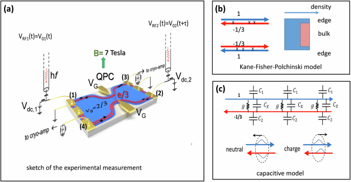
The measurements are performed on a two-dimensional electron gas made in high mobility GaAs/Ga(Al)As heterojunction with electron density ns = 1.11 1015 m−2 and zero field mobility μ = 300 m2 V−1 s−1, see SM. The filling factor ν = 2/3 occurs at field B\(\approx\)7 Tesla. A sketch of the sample with schematic external circuitry is shown in Fig. 1a. DC, low-frequency AC and microwave voltages can be applied to the ohmic contacts (1) and (2). They are used to inject a DC current or photo-excited quasiparticle-quasihole pairs towards a QPC placed at the center of the sample. Contacts (3) and (4) measure the currents transmitted and reflected by the QPC, respectively. The other two contacts are connected to ground. The sample geometry is symmetric and the distance between each ohmic contact and the central QPC is short, ~20 μm, but larger than the expected range of \({l}_{eq}\).
Identifying the nature of the inner edge at filling factor 2/3
Prior to exploring the high-frequency dynamics of the 2/3 edge, we first proceed to identify the nature of the inner-edge, expected to be a counter-propagating “−1/3 edge. This is done by a double determination of the quasiparticle charge e* tunneling between counter-propagating inner edges when they are mixed by the QPC. Two methods are used:
1)
The standard method involves applying only a DC bias voltage to the injecting contact and observing the Poissonian statistics of the backscattering current noise in the WB regime. In this case, the charge e* is equal to the ratio of the current noise power to the mean backscattered current.
2)
A metrological-like method based on comparing a DC bias voltage \({V}_{{DC}}\) to microwave frequency f using the fractional Josephson relation:
$${e}^{*}{V}_{{DC}}=\pm {hf}$$
(1)
where h is the Planck constant and VDC denotes the DC voltages at which the first thermally rounded PASN singularities occur.
Method 1: The so-called DC Shot Noise (DCSN) \({S}_{I}^{{DC}}\left({V}_{{DC}}\right)\) is measured. It represents the increase of the noise with respect to the equilibrium noise due to the partitioning of the charges under a DC bias voltage VDC. No microwave is sent to the sample, but only a DC voltage \({V}_{{DC}}\) is applied on the upper left ohmic contact to inject the current \({I}_{0}=({2e}^{2}/3h){V}_{{DC}}\) towards the QPC. For weak quasiparticles tunneling with charge e* the shot noise is given by refs. 43,44,45:
$${S}_{I}^{{DC}}\left({V}_{{DC}},{T}_{e}\right)=2{e}^{*}{I}_{B}({V}_{{DC}})(1-R)\left(\coth \left({e}^{*}{V}_{{DC}}/2{k}_{B}{T}_{e}\right)-2{k}_{B}{T}_{e}/{e}^{*}{V}_{{DC}}\right)$$
(2)
In the large voltage limit \({e}^{*}{V}_{{DC}} \, \gg \, {k}_{B}{T}_{e}\), the charge e* is given by the ratio of \({S}_{I}^{{DC}}({V}_{{DC}})\) over the backscattering current \({I}_{B}=R({V}_{{DC}}){I}_{0}\) where \(R \, \ll \, 1\) is the reflection probability. Our setup allows two choices for measuring \({S}_{I}^{{DC}}\): the Auto-Correlated Shot Noise (ACSN) \({S}_{{I}_{3}{I}_{3}}={S}_{{I}_{4}{I}_{4}}\) of the transmitted current I3 or the backscattering current I4, or the Cross-Correlated Shot Noise (CCSN) \(-{S}_{{I}_{4}{I}_{3}}\). Both measurements should provide the same information as one expects \({S}_{{I}_{3}{I}_{3}}\left({V}_{{DC}},{T}_{e}\right)={S}_{{I}_{3}{I}_{3}}\left(0,{T}_{e}\right)+{S}_{I}^{{DC}}({V}_{{DC}},{T}_{e})\) and \(-{S}_{{I}_{3}{I}_{4}}={S}_{I}^{{DC}}({V}_{{DC}},{T}_{e})\) as long as \({S}_{{I}_{3}{I}_{3}}(0,{T}_{e})\), proportional to the electronic temperature Te, remains constant. Up to now, most fractional charge determinations at 2/3 were done using the ACSN, see ref. 37. However, the latter may significantly overestimate e* due to electron heating. Indeed, inelastic charge equilibration processes between the 1 and −1/3 channel at 2/3 give an electronic temperature \({T}_{e}\propto {V}_{{DC}}\) originating from “hot spots discussed in ref. 25,26,30, which increases the ACSN. In contrast, the CCSN gives a fair determination of e* as heating effects give only a weak underestimation, see Supplementary Note B for a discussion on ACSN and CCSN.
The ACSN and CCSN measurements are shown in Fig. 2A. For ACSN, the VDC = 0 shot noise has been subtracted for better comparison with CCSN. The upper graph shows that the ACSNs \({S}_{{I}_{3}{I}_{3}}\) and \({S}_{{I}_{4}{I}_{4}}\) measured at 16 mK versus the DC voltage are well above the CCSN \({S}_{{I}_{3}{I}_{4}}\). The red dashed curve is Eq. (2) using e*=e/3 and IB calculated from the simultaneously measured reflection R(VDC) shows good agreement with the CCSN. In contrast, if only ACSN were measured, the charge e* would have been overestimated. The figure below shows similar measurements done at a higher temperature, 110 mK. We observe that ACSN and CCSN merge together, and both measurements provide a correct determination of e*. The bottom graph of panel (A) shows how e* deduced from ACSN and CCSN varies with temperature. As discussed in the Supplementary, we find the variations are consistent with an electronic temperature varying as \({T}_{e}\left(V\right)=\sqrt{{T}^{2}+{\left(\frac{\lambda e{V}_{{DC}}}{{k}_{B}}\right)}^{2}}\) with \(\lambda \approx 0.05\). λ is a non-universal phenomenological parameter that accounts for the Wiedemann–Franz law, which describes the balance between the heat generated by the finite current in the input channel and the finite electronic thermal conductivity. From now on, all current noise measurements presented here will use cross-correlations, which are much more reliable. We note that a recent study (ref. 46) observed the signature of ‘hot spots’ in noise measurements at ν = 2/3, and advocated the use of CCSN measurements at low temperatures. However, no detailed comparison was made between ACSN and CCSN.
Fig. 2: determination of e*.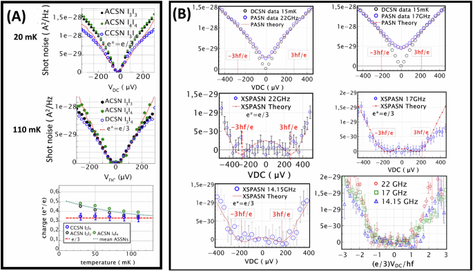
A ACSN (black and green open circle) and CCSN (open blue circles) measured at 16 mK (top graph) and 100 mk (middle graph). The bottom graph shows the apparent evolution of e* measured by ACSN (black and green open circles) and CCSN (blue circles) versus temperature. The dashed line denotes e* = e/3, and the green dashed line is a guide for ACSN variations. B DCSN (open black circles) and PASN (blue circles) measured for 22 (left) and 17 GHz (right) microwave excitation (Vac = 170 and 180 μV). The red dashed curves are fits using Eq. (4) and electronic temperature Te = 75 and 110 mK, respectively. The middle graphs show the corresponding XSPASN for 22 (left) and 17 GHz (right). The minima are found close to the ‘Josephson’ voltages of 272 μV and 210 μV, respectively. For the lowest frequencies, the minima are found to be slightly shifted to a lower value both theoretically and experimentally due to thermal rounding and non-linear IVC. The graph in the bottom left corner shows XSPASN for 14.15 GHz. The bottom right figure plots all XSPASN curves versus voltage in units of 3hf/e on the x axis. Error bars in each figure correspond to the residual Gaussian statistical noise originating from the cryogenic amplifier noise after time-averaging.
Method 2: In a second step, we superimpose on the injecting contact a microwave voltage of amplitude \({V}_{0}\cos (2\pi {ft})\) to the DC voltage \({V}_{{DC}}\). This generates a photo-assisted shot noise, or PASN, predicted to be refs. 47,48,49,50:
$${S}_{I}^{{PASN}}\left({V}_{{DC}}\right)={\sum }_{l=-\infty }^{+\infty }{J}_{l}^{2}\left(\frac{{e}^{*}{V}_{{ac}}}{{hf}}\right){S}_{I}^{{DC}}\left({V}_{{DC}}+\frac{{lhf}}{{e}^{*}}\right)$$
(3)
This Tien–Gordon-like expression is very useful because, knowing the experimental DCSN \({S}_{I}^{{DC}}({V}_{{DC}})\) we can predict the PASN from the photo-absorption probabilities \({J}_{l}^{2}(\frac{{e}^{*}{V}_{{ac}}}{{hf}})\). Here, Jl is an integer Bessel function, and \({V}_{{ac}}\) is the microwave excitation voltage at the QPC. Furthermore, the thermally rounded zero-bias singularity of the DCSN is replicated when VDC is a multiple of the voltage hf/e*, which is a fractional Josephson relation38. This provides a metrological way to determine e*, a method already used to determine the e/3 and e/5 tunneling charges at ν = 2/5 in ref. 39.
Figure 2B shows our experimental PASN measurements used to determine e*. The upper left and right graphs show cross-correlation DCSN (black open circles) and PASN (blue open circles) measurements for microwave frequencies 22 and 17 GHz, respectively. For better reliability, DCSN and PASN measurements are obtained from the CCSN \({-S}_{{I}_{3}{I}_{4}}\). The red dashed curves are best PASN fits from Eq. (3) with e* = e/3 and Vac = 170 μV and 180 μV, respectively. Although the fits are sufficient to confirm that e* = e/3, in order to better visualize the “Josephsonvoltages \(\pm {hf}/{e}^{*}\), we construct the excess PASN (XSPASN) from which the zero-photon absorption/emission part is subtracted:
$${S}_{I}^{XSPASN}\left({V}_{DC}\right)={\sum }_{|l|\ge 1}^{+\infty }{J}_{l}^{2}\left(\frac{{e}^{*}{V}_{ac}}{hf}\right){S}_{I}^{DC}\left({V}_{DC}+\frac{{lhf}}{{e}^{*}}\right)$$
(4)
The XSPASN graphs for 22 GHz and 17 GHz are displayed below their respective PASN graphs. Local XSPASN minima give the loci of the “Josephson voltage associated with charge e*=e/3. The lower left graph shows a similar XSPASN curve for a lower microwave frequency of 14.15 GHz. All XSPASN curves are rescaled in the lower-right figure, with e*VDC/hf used as the x axis.
In a recent theoretical work51, the simultaneous tunneling of anyon of charge e/3 and 2e/3 is considered. The authors showed that even a few % relative amount of 2e/3 tunneling charge can be observable as a secondary XSPASN minima at voltages \(\pm 3{hf}/2e\) in addition to the main \(\pm 3{hf}/e\) minima. Within our experimental noise uncertainty, no 2e/3 charge tunneling is detectable.
To conclude this part, method 2 provides an unambiguous determination of an e/3 tunneling charge at 2/3 and, within our uncertainty, eliminates the possibility of a few % concomitant tunneling of charge 2e/3. Method 1 resolves the puzzling larger e* values previously observed at low temperatures due to the use of ACSN measurements alone. The electron heating model presented in the Supplementary Part B provides a rational explanation for the artefacts of DC shot noise charge measurements at 2/3.
2/3 edge-channel dynamic model
Now that we have identify e* and therefore the fractional nature of the inner edge, we can address the dynamics of the 2/3 edge. As a guide, we use the incoherent inter-channel tunneling model developed in refs. 25,26,27,28,29. characterized by a constant distributed tunneling conductance \(g=\frac{{e}^{2}}{2h{l}_{{eq}.}}\) of electrons between the 1 outer channel and the −1/3 edge channel. In the Luttinger Liquid (LL) approach, the tunneling element g is expected to depend on the difference between the local electrochemical potentials of the inner and outer edge states. However, when the microwave voltage amplitude applied to the injecting Ohmic contacts is small, specifically \({V}_{0}\ll 2\pi {k}_{B}{T}_{e}/e\) (where Te is the electronic temperature), we can approximate g as a phenomenological constant. To describe the edge dynamics, we follow ref. 32. which solves the collective modes of the 2/3 edge in a transmission line model. Instead of considering the inter-mode coupling and the intra-mode interaction as phenomenological parameters as done in standard cLL models, ref. 32. uses realistic parameters where the interaction can be modeled by capacitances32,52,53,54 see Fig. 1c. The equation of motion of the current can be written as follows:
$$\frac{\partial }{\partial t}\vec{{{\boldsymbol{I}}}}=-{{\boldsymbol{\sigma }}}{{{\boldsymbol{C}}}}^{-{{\bf{1}}}}\frac{\partial }{\partial x}\vec{{{\boldsymbol{I}}}}–{{\boldsymbol{\sigma }}}{{{\boldsymbol{C}}}}^{-{{\bf{1}}}}{{\boldsymbol{g}}}{{{\boldsymbol{\sigma }}}}^{-{{\bf{1}}}}\vec{{{\boldsymbol{I}}}}$$
(5)
where \(\vec{{{\boldsymbol{I}}}}=\left(\begin{array}{c}{I}_{1}\\ {I}_{2}\end{array}\right)\), with \({I}_{1\left(2\right)}\left(x,t\right)\) denoting the current in outer (inner) channel at time t and point x, \({{\boldsymbol{\sigma }}}={\sigma }_{q}\left(\begin{array}{cc}1 & 0\\ 0 & -1/3\end{array}\right)\) accounts for the channel conductance with \({\sigma }_{q}={e}^{2}/h\), \({{\boldsymbol{g}}}=g\left(\begin{array}{cc}1 & -1\\ -1 & 1\end{array}\right)\) describes the inter-channel tunneling conductance and \({{\boldsymbol{C}}}=\left(\begin{array}{cc}{C}_{1}+{C}_{X} & -{C}_{X}\\ {-C}_{X} & {C}_{2}+{C}_{X}\end{array}\right)\) the interaction, with C1(2) the outer (inner) channel self-capacitance per unit length and CX the inter-channel capacitance per unit length. In the absence of inter-channel conductance, Eq. (1) is equivalent to that used in the K-F-P model for cLL bosonization (see SM). In the following, we will use realistic parameters with \({C}_{1}={C}_{2}=\) 0.1 nF/m and \({C}_{X}=\) 0.4nF/m as in ref. 32. Variations around these parameter values do not qualitatively change the predictions. Here, we used geometric capacitances in Eq. (1) instead of electrochemical capacitances \({\widetilde{C}}_{1(2)}\) as, in GaAs 2DEG, we can safely neglect the contribution of quantum capacitances \({c}_{q,1(2)}\,\), with \(\frac{1}{{\widetilde{C}}_{1(2)}}=\frac{1}{{C}_{1(2)}}+\frac{1}{{c}_{q,1(2)}}\). This would not be the case for Graphene 2DEGs for which the high Fermi velocity leads to a non-negligible quantum capacitance contribution.
Equation(5) describes the propagation of the coupled modes with possible decay due to the tunneling conductance. We seek a solution of the form \(\left(\begin{array}{c}{I}_{1}(x,t)\\ {I}_{2}(x,t)\end{array}\right)=\left(\begin{array}{c}{I}_{1}\\ {I}_{2}\end{array}\right)\exp i({kx}-\omega t)\). The local electrochemical potential expressed in units of voltage are related to the local current via \({V}_{1}\left(x,t\right)={I}_{1}(x,t)/{\sigma }_{q}\) and \({V}_{2}\left(x,t\right)=-3{I}_{2}(x,t)/{\sigma }_{q}\). The diagonalization of (5) gives two eigenmodes labeled (I) and (II). Solution (I) corresponds to a downstream mode, i.e. with \({{\rm{Real}}}\left({k}_{(I)}\right)={k}_{(I)}^{{\prime} } > 0\) and weak decay \({\mathrm{Im}}\left({k}_{(I)}\right)={k}_{\left(I\right)}^{{\prime} {\prime} }0\). The mode is close to a charge mode with the inner and outer channel voltages almost in phase, i.e. \({V}_{1}\left(x,t\right)\cong {V}_{2}\left(x,t\right)\). Solution (II) correspond to an upstream mode, i.e. with \({{\rm{Real}}}\left({k}_{({II})}\right)={k}_{({II})}^{{\prime} } < 0\) and strong decay \({{\rm{Im}}}\left({k}_{({II})}\right)={k}_{({II})}^{{\prime} {\prime} } < 0\). The mode is almost neutral \({V}_{1}\left(x,t\right)\cong {-V}_{2}\left(x,t\right)\) with inner and outer voltage almost out of phase. The decay lengths \(1/{k}_{\left(I\right),({II})}^{{\prime} {\prime} }\) ”or each mode are plotted in Figs. S4b and S5b of the Supplementary. Because the outer and inner channel voltages are out of phase, a large inter-edge tunnel current leads to a strong attenuation of the neutral mode. Indeed, we find \(\frac{1}{{k}_{\left({II}\right)}^{{\prime} {\prime} }} < {l}_{{eq}.}\) at all frequencies. Consequently, the K-F-P neutral modes cannot propagate beyond the charge equilibration length. In the seminal work of K-F-P the charge mode dynamics were considered, but the extremely strong decay of neutral modes was not discussed. As recently shown in ref. 30., it is likely that their role has been overestimated in the previous literature31. In contrast, mode (I), having in-phase inner and outer channel voltages, is associated with little inter-channel tunneling, leading to large distance propagation. An important parameter is the cross-over frequency:
$${f}_{C.0.}=\frac{1}{2\pi }\frac{{e}^{2}}{2h{C}_{X}{l}_{{eq}.}}\cong \frac{7.7{GHz}}{{l}_{{eq}.}[\mu m]}$$
(6)
For \(f \, \ll \, {f}_{C.O.}\), the inter-channel coupling is dominated by tunneling, and one can neglect the Coulomb coupling, while for \(f \, \gg \, {f}_{C.O.}\) interaction dominates and tunneling is negligible. For frequency in the vicinity of \({f}_{C.O.}\) one expects important changes in the frequency response of the 2/3 edge. We anticipate dispersive effects that will alter the shape of the charge pulse, which can be investigated using HOM shot noise measurements. This is shown in Fig. S4a, where the computed phase velocity of the charge mode is plotted versus frequency. We also expect strong variations of the frequency-dependent attenuation of the charge mode, also affecting charge pulse propagation, see Fig. 3c in the main text and S4(b) in the SM.
Fig. 3: Measuring de charge mode attenuation on the 2/3 fractional edge.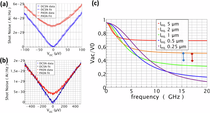
a, b show DCSN and PASN measurements using f = 15.3 GHz microwave excitation on contact (1) versus DC bias voltage. aν = 2: inner edge weakly backscattered, transmission D = 0.96 ± 1%. The graph shows the experimental cross-correlated DCSN and PASN amplitude versus DC voltage (blue and red circles, respectively). The blue and red dashed curves are fits based on Eq. (2) and Eq. (3) for DCSN and PASN with e* = e and, respectively Te = 31.0 ± 1.5 mK and 95 ± 5 mK. Equation(4) gives Vac(ν = 2) = 70.1 ± 3 μV (e* = e) for −6 dBm rf source power; bν = 2/3: inner-edge transmission 0.98. DCSN and PASN data are taken for double Vac microwave amplitude (+6 dBm rf source power) to compensate for the lower tunneling charge e* = e/3. The DCSN and PASN fits give, respectively Te = 29 ± 1.5 mK and 183 ± 9 mK and Vac(ν = 2/3) = 143 ± 3 μV for; c charge mode amplitude reduction Vac/V0 expected for ν = 2/3 after the 20 μm contact-to-QPC propagation length and calculated for various \({l}_{{eq}.}\) using the model given by Eq. (5). The short blue vertical line corresponds to the range of the Vac (ν = 2/3, +6 dBm) reduction found between 0.50 and 0.41 for the present 15.3 GHz drive. The red vertical segment is the reduction between 0.48 and 0.40 found at 17.05 GHz, see SM. We estimate 1 μm \(\le {l}_{{eq}.}\le 2\)μm.
PASN measurements
We first present PASN measurements to probe the quasiparticle of the inner “-1/3” channel and estimate the charge mode attenuation. Then we will show the results of electronic HOM shot noise measurements.
Figure3 shows PASN measurements done at ν = 2 and ν = 2/3 at microwave frequency f = 15.3 GHz. Comparing the Vac amplitudes deduced from the PASN fits of Fig. 3a, b the attenuation Vac(ν = 2/3)/V0 at ν = 2/3 can be estimated ranging between 0.5 and 0.41, respectively, assuming no or, more likely, 10% charge mode attenuation at ν = 2. Figure 3c shows the expected attenuation versus frequency computed from the solutions of Eq. (5) for various \({l}_{eq}\). The range of attenuation measured at 15.3 GHz is indicated by the blue vertical segment. Similar measurements taken at 17.05 GHz are indicated by a red segment, see Supplementary Note D1. Comparing our data with the model provides an estimation of the charge equilibration length 1 μm \(\le \,{l}_{{eq}.}\le\)2 μm. The present estimation is reasonable as it is found to be weakly dependent on the actual value of the coupling capacitance, CX, which may vary depending on how sharply the 2DEG is confined laterally.
Electronic Hong Ou Mandel measurements
Here, the goal is to further probe the above model by checking for the expected deformation of narrow charge pulses due to inter-channel tunneling between counter-propagating edge channel at ν = 2/3. The reason for pulse shape deformation is twofold. Figure 3c shows that, at ν = 2/3, the attenuation of the charge mode is stronger at a large frequency than at a lower frequency. Thus, cutting the high-frequency components is likely to broaden narrow pulses. Another reason is the dispersive effect arising from the charge pulse phase velocity, which shows a pronounced variation for a wide frequency range around the cross-over frequency \({f}_{C.0.}=\frac{1}{2\pi }\frac{{e}^{2}}{2h{C}_{X}{l}_{{eq}.}}\), see Fig S4a in the Supplementary. In contrast, for ν = 2 or 3, co-propagating channels and rare inter-channel tunneling mixing points are expected to preserve the overall shape of narrow pulses while they propagate along the 20 μm long distance from the injecting contact to the QPC.
To proceed, we generate periodic Lorentzian pulses with 5 GHz repetition frequency. This is done using an RF-source generating the four first harmonics, coherent in phase and exponentially decreasing in amplitude, whose sum accurately approximates Lorentzian pulses with tunable width55,56,57, namely 36 ps and 72 ps, see SM.
We first perform the HOM shot noise experiment at integer filling factors ν = 2 and 3, see Fig. 4a, b, respectively. This provides a convenient benchmarking of the quality of the pulse sent on the sample, as we do not expect significant deformation along integer edges. Indeed the measurements show clear HOM dips whose width at half amplitude is consistent with a doubling of the 36 ps width (as HOM variation can be viewed as a kind of pulse convolution, see Supplementary Note D2 and HOM measurements in ref. 56). We note however that the periodic HOM noise variation, with period 1/f = 200 ps does not show a single HOM dip centered at time delay τ = 0 but a weaker replica around τ = 95 ps. The origin of the multiple HOM dips has been discussed in ref. 58,59 and attributed to a few discrete inter-channel tunnel mixing points. For a unique mixing point localized between the injecting contact and the QPC in each input channel, the general expression is of the form \({Cst}+A{S}_{{HOM}}\left({\Delta }_{13}\right)+B{S}_{{HOM}}\left({\Delta }_{23}\right)+C{S}_{{HOM}}\left({\Delta }_{14}\right)+D{S}_{{HOM}}({\Delta }_{24})\) where \({S}_{{HOM}}\left(.\right)\) is the generic HOM noise of two colliding Lorentzian pulses and Δi,j denotes various propagation time-delays. The pre-factors (A-D) are related to the QPC transmission and the tunneling point mixing amplitudes in each input arms, see Supplementary Note D2. In Fig. 4a, we show the measured HOM noise and a fit using the previous form. This confirms that the HOM dips are not broadened but simply duplicated as predicted in refs. 58,59. A detailed study at ν = 2, will be published elsewhere51. Similar features are shown in Fig. 4b for ν = 3 for which discrete mixing points are also expected to lead to multiple HOM dips. Figure 4c shows the HOM noise at ν = 2/3. In contrast to Fig. 4a, b no narrow HOM dips are observable but only an asymmetric broad variation versus the time delay τ. Indeed, Fig. 4d shows the simulation of the shape of Lorentzian pulses injected at the ohmic contact (black dashed curve) and after their propagation along the 2/3 edge towards the QPC over the 20 μm length. The curves are computed for \({l}_{{eq}.}\) = 2 μm (left) and 0.25 μm (right). They show increasing broadening and deformation for smaller \({l}_{{eq}.}\) as expected from high-frequency attenuation and dispersive effects.
Fig. 4: Hong Ou Mandel interference of the e/3 anyons of the ν = 2/3 edge channel.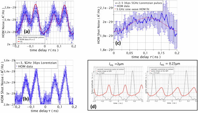
Lorentzian pulses of 36 ps full width at mid-height are periodically injected at 5 GHz repetition frequency on opposite contacts with a relative time delay τ and the cross-correlated noise is measured. a Absolute value of the negative HOM cross-correlated noise versus time delay at filling factor ν = 2. To better appreciate the variations, the data taken for 0 < τ < 0.2 ns have been replicated by a negative shift of one period. Multiple dips within the single period (T = 0.2 ns) can be described by split, undeformed Lorentzian pulses. (red dashed line fit) according to refs. 49,50. The fit uses four Δi,j: τ−20 ps, τ-97 ps, τ−150 ps, τ−27 ps, known modulo 200 ps, see Supplementary Note D2. b same for ν = 3. c HOM noise of the e/3 fractional excitations observed at ν = 2/3. The absence of narrow dips and a single broad variation against τ confirms the small \({l}_{{eq}.}\) and the dispersive effect predicted by the model. The red dashed curve is a tentative HOM noise fit where the deformed pulses have been approximated to a 5 GHz sine-wave. d computed pulse deformation (red curves) for 20 μm propagation length and \({l}_{{eq}.}\) = 2 μm (left graph) and 0.25 μm (right graph). Note the absence of neutral mode because of strong decay. As a reference, the black dashed curves correspond to the Lorentzian voltage pulse injected on the ohmic contact before propagation. Error bars in each figure correspond to the residual Gaussian statistical noise originating from cryogenic amplifier noise after time-averaging.
In summary, exploiting microwave photo-assisted shot noise, our measurements provide the unambiguous determination of the tunneling charge at filling factor 2/3, while showing that DC shot noise approaches are unable to provide reliable e* determination at 2/3, solving the long-standing puzzle of e* increasing above e/3 at low temperatures. Microwave photo-assisted shot noise and two-particle dynamical interferometry offer insights into the charge dynamics of the ν = 2/3 edge at a mesoscopic scale. They also provide a practical estimate of the charge equilibration length \({l}_{{eq}.}\), beyond which anyon braiding interferometry is likely to be unfeasible. Our findings align with models predicting that K-F-P neutral modes cannot propagate beyond \({l}_{{eq}.}\) prompting a reevaluation of the role of neutral modes in previous experimental studies where \({l}_{{eq}.}\) is significantly shorter than the relevant sample dimensions. Our approach is versatile and can be applied to a variety of quantum Hall phases exhibiting counter-propagating edge or interface60 modes, including those hosting non-Abelian anyons, as well as to other topological 2D materials at various filling factors.