

Local optoelectronic detection of discrete exciton Rydberg states
We first introduce the ER-MIM technique that enables us to sense excitons using photoelectrical effects at the nanoscale. As shown in Fig. 1a, our setup consists of two parts: a microwave transmission line impedance-matched to a metallic scanning probe (tip)27,28,29, and a continuously wavelength-tunable laser that is fiber-coupled into a Helium-3 cryostat and illuminates the tip. The real and imaginary parts of the reflected microwave signals are recorded, which are in- and out-of-phase with the reference microwave excitation line, respectively. Our measurements were conducted at ~1.5 K and 3 GHz, yet this method can readily be adapted to even lower temperatures (e.g., the base temperature of the Helium-3 cryostat).
Fig. 1: Sensing exciton Rydberg states at the nanoscale.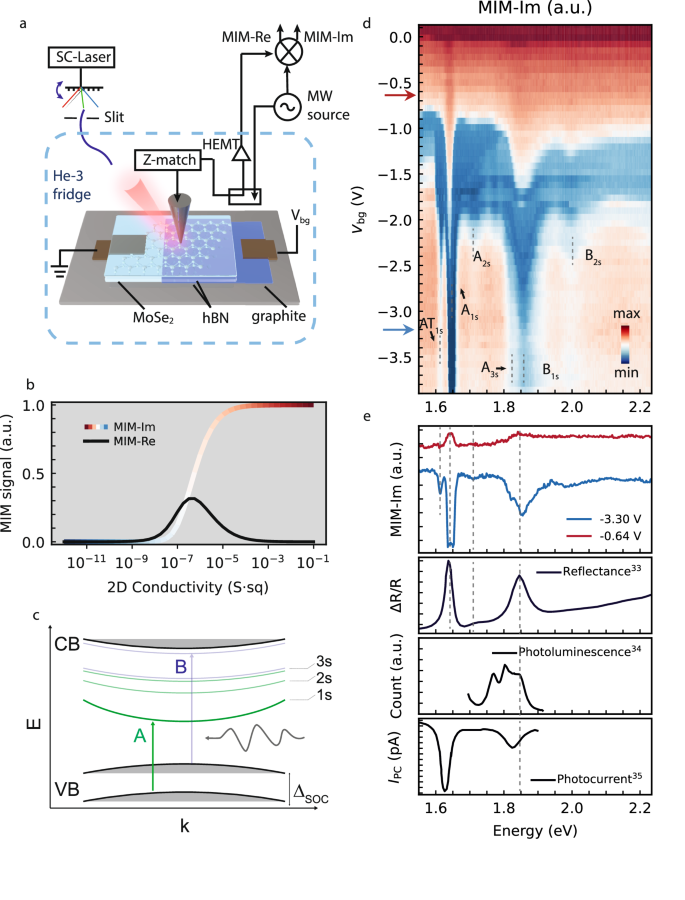
a The experimental setup of the exciton resonant—microwave impedance microscopy (ER-MIM) measurements. The optical source is a supercontinuum laser. b The response curves of MIM-Im (imaginary part) and MIM-Re (real part) as a function of the sheet conductivity of MoSe2. In the MIM-Im curve, the colormap was selected such that blue indicates lower conductivity and red indicates higher conductivity. In MIM-Im colorplots, we will refer to the two saturated signal regimes, the smallest and largest conductivity, as “mim” and “max,” respectively. c A schematic showing relevant energy levels and optical transitions forming 1s, 2s, and 3s Rydberg states of A and B excitons in monolayer MoSe2. d ER-MIM-Im signal as a function of back gate voltage Vbg and optical excitation energy. The blue and red arrows on the y axis correspond to two representative doping levels. e Comparison of ER-MIM results (at the two doping levels marked in (d) with spectra from three widely used far-field optical techniques: optical reflectance33, photoluminescence34, and photocurrent35 measurements.
Qualitatively, the underlying mechanism of using MIM to study materials is that its real (in-phase) and imaginary (out-of-phase) parts of the reflected microwave signals reflect the degree of dissipation and microwave screening by the sample, respectively. In this study, we focus on the imaginary component (MIM-Im). Since highly conductive materials provide strong microwave screening, yielding the largest MIM-Im response in a reflection geometry, whereas insulating materials give minimal screening and thus exhibit a much smaller MIM-Im signal, the local conductivity of the material can be inferred from the MIM-Im measurement. In Fig. 1b, we present two calculated response curves that illustrate the relationship between the real (in-phase) and imaginary (out-of-phase) parts of the reflected microwave signals and the local complex conductivity of the sample.
The material we study is a prototypical 2D TMD device, a monolayer of MoSe2 encapsulated within hBN layers with graphite as a back gate. The optical spectrum of monolayer MoSe2 possesses a series of pronounced resonances, categorized as A- and B excitons (see Fig. 1c). These excitons arise from two optical transitions involving states in the upper and lower energy spin valence bands. They possess Rydberg atom-like energy levels, each designated by its principal quantum number, n.
We track the evolution of the microwave response as a function of excitation wavelength and back gate voltage Vbg controlling the free carrier density in MoSe2 (imaginary part of the ER-MIM signal shown in Fig. 1d). The blue and red colored regions in this 2D plot correspond to low conductivity (e.g., 2D conductivity close to 10−7 S sq) and high conductivity (e.g., 2D conductivity close to 10−4 S sq) of MoSe2, respectively, with the colorbar in direct correspondence with the one in Fig. 1b. The overall dependence of conductivity on back gate voltage agrees with the transfer curve of a semiconductor, i.e., it decreases when crossing from the conduction band into the bandgap, and increases when entering the valence band. On top of this overall trend, at specific photon energies (e.g., 1.65 eV), the conductivity has an extra increase at smaller ∣Vbg∣ (e.g., <2V), and another decrease at large ∣Vbg∣ (e.g., >2 V). We identify those photon energies as in resonance with neutral A1s and B1s excitons, and the excited Rydberg states including A2s, A3s, and B2s, as well as weaker modulations in intensity features corresponding to their charged counterparts like AT1s and AT2s (which are usually referred to as trion or exciton polaron, and their distinction will be discussed below).
The changes in ER-MIM-Im signal near excitonic resonances imply the observation of photoconductivity associated with exciton formation. The relative change of conductivity on exciton resonance (compared to off resonance) changes from positive at small ∣Vbg∣ to negative at large ∣Vbg∣, and can be attributed to two major processes (a discussion on ruling out other possible optical processes in supplementary note 2). One is the photoconductive effect27, where the exposure of TMD-based devices to light generates neutral electron-hole pairs. Then, the trapping of one carrier and the release of the other free carrier from an exciton could result in an enhanced conductivity30. This process explains our observation of positive conductivity near excitonic resonances. The other is Auger-assisted tunneling effect31,32 (also see Fig. S2). When the photon energy is in resonance with the binding energy of excitons, a generated exciton can excite a free hole when it recombines during the Auger process. The hole can subsequently tunnel through the hBN barrier to reach the bottom gate. When many free carriers escape the sample, the carrier density reduction effectively reduces the MoSe2 conductivity. Since the energy barrier on the hole side between MoSe2 and hBN is much smaller than the electron side, the decrease in conductivity upon photoexcitation is only observed when MoSe2 is hole-doped. We further examined monolayer WSe2, and the result is consistent with this argument (Fig. S2). Therefore, the conductivity decrease at large ∣Vbg∣ in our measurement is attributed to the dominance of the Auger effect.
We further compare two linecuts of ER-MIM-Im spectrum with previously reported far-field spectra of excitons in monolayer MoSe2 (Fig. 1e). The red and blue curves show excitonic peaks and dips, highlighting the signal from the photoconductivity and Auger-assisted tunneling effects, respectively. The comparison reveals excellent agreement between the identified exciton energies in ER-MIM-Im and the results obtained from optical reflectance33, photoluminescence34, and photocurrent35 measurements. It is noteworthy that our spectral resolution stands on par with, or surpasses, those of the above-mentioned area-averaged methods. This compelling correspondence demonstrates that our ER-MIM technique enables accurate photoelectric measurements of exciton spectra with the added benefit of exceptional spatial resolution and access to a temperature regime that has, until now, been unattainable.
The interplay between excitons and the charge environment
To untangle the exciton-electron interactions at the nanoscale, we modulate carrier density of MoSe2 by controlling Vbg applied onto graphite while collecting ER-MIM spectra (Fig. 1a). The graphite boundary splits MoSe2 into three distinct spatial regions (Fig. 2a): (I) a region that extends beyond the graphite back gate (BG) that is ungated, (II) the region directly above the BG, in which the carrier density is controlled by Vbg, and (III) the depletion region associated with the nanojunction between regions I and II. Our focus lies on contrasting the ER-MIM responses in regions I and II, which are distant from the junction and hence less influenced by the electric field, yet differentiated by their carrier densities. Such a comparative approach enables a systematic exploration of excitonic behaviors in diverse local charge environments.
Fig. 2: The interplay between exciton behaviors with local charge environment.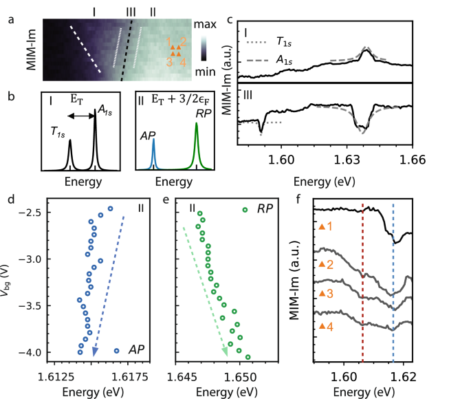
a A MIM map showing the MoSe2 sample (flake boundary outlined by a white dashed line) partially on top of a graphite back gate (boundary outlined by a black dashed line). The device can be divided into three regions: I (outside of graphite), II (above graphite), and III (depletion region, with boundaries outlined by two white dotted lines). Scale bar: 500 nm. b Schematics of the exciton and trion spectra (left), and the exciton-polaron spectra (right). c The ER-MIM-Im spectrum measured in region I (top panel) and III (bottom panel). The gray dashed and dotted lines are fittings of A1s exciton and T1s trion. d The evolution of eigenenergy of the A exciton: the blue dotted line is the attractive branch AP. e The evolution of the repulsive polaron branch of the A exciton, as shown by the green dashed line. f ER-MIM-Im spectra measured at four locations in region II with a fixed gate voltage. The locations are marked by four orange triangles a. The blue dotted line is AP, while the red dashed line denotes an extra feature.
Figure 2b depicts two scenarios of exciton-electron interactions. The first involves trions, charged and weakly coupled three-particle complexes formed by binding two electrons (or holes) to one hole (or electron). Trion and exciton eigenenergies differ by the trion binding energy, denoted as ET (left schematic). The second scenario features charge-neutral bosons resulting from excitons interacting with the degenerate Fermi sea of excess charge carriers (right schematic). In this context, excitons become dressed by Fermi sea excitations, giving rise to attractive and repulsive exciton-polaron (AP and RP) quasiparticles, akin to Fermi-polarons in the context of cold atoms11,34. The energy difference between AP and RP branches, or the exciton polaron binding energy, is ~ET + 3/2ϵF, with ϵF representing the Fermi energy11. To examine these two physical pictures, we take advantage of the sensitivity of ER-MIM spectra to ϵF (gate)-tunable local excitonic energy levels.
In the upper panel of Fig. 2c, we present the ER-MIM spectrum obtained in region I. This region is not strongly affected by the back gate voltage, hence close to intrinsically (n-)doped. The spectrum reveals one major resonance feature at ~1.642 eV, corresponding to exciton A1s (fitting shown as a gray dashed line). Notably, at 1.5 K, the linewidth of the exciton A1s dip is ~2.5 meV, closely approaching the theoretically calculated intrinsic linewidth of excitons36. Similar linewidth was observed in the spectrum measured in the more p-doped region III (shown in the lower panel of Fig. 2c). The spectrum shows one more prominent feature centered at ~1.59 eV, corresponding to trion T1s (fitting shown as a gray dotted line).
On the other hand, we measured the back gate dependence of the ER-MIM spectra sitting at a spot in region II. This region has the highest carrier density among the three. The blue circles in Fig. 2d are extracted exciton eigenenergies at different Vbg near formerly designated T1s, and the green circles in Fig. 2e are another eigenenergy near formerly designated A1s. The red dashed and blue dotted T1s branches display nearly linear redshifts, while the A1s exciton energy demonstrates a linear blueshift with Vbg. This trend remains consistent throughout the range of Vbg in our experiments. The increasing energy separation between the branches in Fig. 2d, e is a signature of exciton-polaron (RP) formation at elevated carrier doping levels (Fig. 2b). In this framework, the formerly assigned A1s becomes repulsive RP. The T1s branch turns into an attractive exciton polaron (AP).
The observed gate-dependent shifts in AP and RP eigenenergies indicate interactions between excitons and free carriers. These energy shifts exhibit an almost linear dependence on Vbg, reflecting a collective effect of carrier density-dependent exciton binding energy change, quasiparticle bandgap renormalization, and the variation of binding energy of the exciton polaron. To quantify the shifts, we introduce a coefficient β, where δE = βn, with δE being the change of eigenenergy of an exciton polaron state, which has a linear dependence on carrier density n. The observed nanoscale spatial variation of δE suggests that the eigenenergy changes can be used as a sensitive local indicator of the charge environment.
Another observed feature is the presence of multiple wiggle-like structures near the attractive exciton polaron energy at various spatial locations (spots 1,2,3,4 shown in Fig. 2a), as shown in Fig. 2f. We further identified that these appear in cases where the ER-MIM signal exhibits more than one feature in its dependence on back gate voltage (Fig. S3), i.e., when the system transitions from insulating to conductive and back to insulating. Such wiggles are indicative of mid-gap states. Since it is very local, this suggests that the observed wiggle-like feature is closely linked to spatial inhomogeneity in the local charge carrier density (from a mix of intrinsic and extrinsic defects like vacancies, impurities and adsorbates). While this effect is often obscured in far-field measurements, mid-gap states have been previously reported in scanning tunneling microscopy studies37. Given our spatial resolution of ~50 nm, both local conductivity variations and exciton energy dispersion are clearly resolved in the ER-MIM signal (also see Figs. 1d and 3c).
Fig. 3: The interplay between exciton behaviors and electric environment.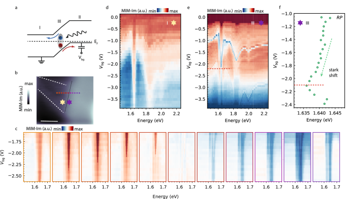
a A schematic of the p-n junction formed through Vbg modulation in region II, and the depletion region formation in III. b MIM-Im image showing the sample geometry, with colored circles and stars marking different locations of further measurements. (The same region as Fig. 2a but at a larger scale, with the MoSe2 flake boundary outlined by white dashed lines, and the graphite boundary outlined by a black dashed line.) Scale bar: 500 nm. c A series of ER-MIM-Im measurements at the locations specified by the colored circles in b. The colors of the boxes are in correspondence with the color of the circles (plots ordered in the sequence from left to right). d ER-MIM-Im measured at the yellow star in b. e ER-MIM-Im measured at the purple star in b. f The extracted repulsive polaron eigenenergy as a function of back gate voltage. The red dashed lines in (e, f) mark the Vbg at which the RP exciton energy has a sudden blueshift.
The interplay between excitons and the electric environment
In addition to the charge environment, to understand the intricate interplay between excitons and the local electrical variations, we examine more closely the ER-MIM signals in region III, the depletion area. Here, an in-plane electric field propels electrons and holes towards regions I and II, respectively. We also compare the excitonic response close by and farther away from the controlled p-n junction, i.e., region III and region II, as illustrated in the schematic in Fig. 3a.
To start with, a systematic ER-MIM scan across the p-n junction was carried out as a function of Vbg and excitation energy. We mark the locations in Fig. 3b and plot the results in Fig. 3c. It is evident that a continuous variation in the ER-MIM-Im signal near the A1s AP and RP resonances is observed across the p-n junction. Especially, when on resonance, there is a continuous change from an increase in conductivity to a decrease, from the left-hand side of the nanojunction to the right-hand side. This marks the conversion from a photoconductive effect-dominated mechanism in the ungated region of MoSe2 to Auger tunneling-dominated mechanism in the back-gated region of MoSe2.
The field effect is then studied in greater detail via high-resolution imaging in region III (Fig. 3d, e, with locations marked by stars in Fig. 3b). The two gate-dependent spectra in region III both appear to be very different from the ones obtained from region II (Fig. 1b). They feature mostly an increase in conductivity at excitonic resonances (red colored regions), and less change with gating. Within region III, measurement in the right part (purple star in Fig. 3b, e) shows a relatively more effective gating effect, where the restoration of some reduction of conductivity due to exciton dissociation-assisted hole tunneling can be identified. This observation further elucidates the p-n junction behavior in region III.
To study the excitonic response to the electric field, we extracted the RP eigenenergy from Fig. 3e, and plotted it in Fig. 3f. There are two distinct features that differ from region II (Fig. 2f): the RP energy exhibits an overall redshift behavior with doping level, instead of a blueshift; the RP energy has an abrupt blueshift at Vbg ~ −2.2 V. The first feature agrees with the dc Stark effect of excitons: δE = −αF2/2, where α is the exciton polarizability12, F represents the electric field strength, and δE signifies the energy shift. The second feature underscores the nonlocal effect of the dielectric constant on exciton energies. Since a carrier density gradient exists in this region, when the right part of the sample goes across the band edge, it leads to a sharp increase in carrier compressibility \(\frac{1}{{n}^{2}}(\frac{\partial n}{\partial \mu })\) (n being carrier density, and μ being the chemical potential), which then changes the exciton screening in the left part. This is consistent with the Coulomb potential screening of excitons through a free electron gas, which leads to another describable dependency of excitons on the environmental permittivity: E = E(κ). These observations suggest how excitons can serve as imaging tools for a p-n junction and reveal intricate nanoscale parameters such as electric field and dielectric constant.
Quantitative photoelectrical imaging and exciton-facilitated electrometry
To quantitatively analyze the ER-MIM data and utilize it for predicting material properties, we developed a deep neural network (DNN)38,39,40,41,42 based on a set of MIM maps. These maps consist of 256 × 100 pixel images, obtained with variations in optical excitation energies and back gate voltages within a 1 μm × 1 μm region at the graphite back gate boundary. Due to the complex, multidimensional nature of the datasets, traditional fitting approaches prove to be inadequate. In Fig. 4a, we present three representative sets of MIM-Im and MIM-Re data collected at Vbg = −3 V, under different conditions: with the light off, under 1.651 eV light excitation, and 1.655 eV light excitation. The 1.651 eV excitation is off-resonance with excitons, while the 1.655 eV excitation is close to the resonance of the RP branch of the A1s exciton.
Fig. 4: Holistic electrical sensing with excitons.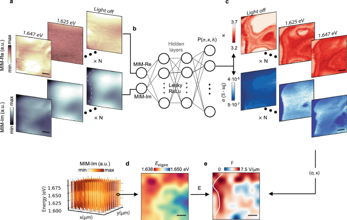
a Representative sets of MIM-Re and MIM-Im images measured with light off, 1.625 eV (away from exciton resonance), and 1.647 eV (close to A1s repulsive exciton-polaron resonance), in a 1 μm × 1 μm region. The white dashed line denotes the graphite boundary. Scale bar: 200 nm. b The deep neural network architecture. c The deep neural network training result of permittivity κ, conductivity σ, for the three columns of MIM data in a. Scale bar: 200 nm. d Left: the ER-MIM-Im hyperspectra as a function of excitation energy and spatial location collected on a 9 × 9 grid. Right: the interpolated exciton eigenenergy extracted from the hyperspectra. Scale bar: 200 nm. e The interpolated in-plane electric field strength prediction based on Eq. (1), and the input from (σ, κ) in c and E in d, as indicated by the black flow arrows. The white dotted line denotes the graphite boundary. Scale bar: 200 nm.
In the following, we show how to use this DNN to predict the local environment (σ, κ, h), i.e., sheet conductivity of MoSe2, the relative permittivity of the hBN-MoSe2-hBN stack, and relative tip-sample distance h, for a given MIM data set. We construct a feedforward network (Fig. 4b), with the inputs being MIM-Re and MIM-Im, either from the experiment or finite element simulations43, and predict the probability at each set of discretized (σ, κ, h) values. We train the network with a total of 64,000 sets of simulation data, which is divided into bins along the σ, κ, and h directions. Each data point is encoded into a 3840-dimensional vector with the elements being its bin membership –1 for a member and 0 for a non-member. Given the absence of a direct correlation between MIM-Re and MIM-Im, and (σ, κ, h), we adopt a Binary Cross-Entropy loss function. In this way, we transform the prediction into a classification problem, where the network output represents the probability for each bin. A good agreement is found between the deep neural network outputs and the ground truth (Fig. S4).
We then apply the trained network to predict the probability distribution of (σ, κ) for a given set of MIM maps in Fig. 4a. The results of (σ, κ) are shown in Fig. 4c. The obtained κ maps indicate the presence of local dielectric disorder in the environmental permittivity, as well as permittivity change of MoSe2 upon back gate doping and optical excitation. The obtained σ maps present the spatially dispersive photoconductivity from the RP exciton polaron. These quantified (σ, κ) maps hence provide a direct measure of the local environment of excitons.
Following the quantification of (σ, κ) maps and our understanding of the exciton eigenenergies variation due to charge and electrical environment, as discussed in the last two sections, we formulate the subsequent expression to describe the local exciton eigenenergy E (also see supplementary information):
$$E={E}_{0}(\kappa )+\beta n-\frac{1}{2}\alpha (\kappa ){F}^{2}.$$
(1)
The first term of the expression, E0, represents the exciton eigenenergy for monolayer MoSe2 under the influence of environmental permittivity, without further considering exciton-electron interactions or electric field effects. The second term represents the interaction between the exciton and free carriers. The variable n corresponds to carrier density, and β is a fitting coefficient. The linear relationship is extracted from experimental results, such as Fig. 2f, and the coefficient β is derived from the back gate sweeping data. Since this term results from a combination of both bandgap renormalization and the reduction in exciton binding energies with carrier doping, and these effects largely cancel each other out, it is not a main contribution to spatial eigenenergy fluctuation. The third term accounts for the Stark effect resulting from in-plane electric fields with strength F. The contribution from out-of-plane electric field is negligible since the in-plane exciton polarizability α is approximately two orders of magnitude larger than the out-of-plane value due to hBN dielectric screening44. In our measurements, the Stark shift term dominates the spatial variation of exciton eigenenergy E.
Subsequently, we determine the exciton eigenenergies E on the 2D grid within the same 1 μm × 1 μm region, through fitting and interpolating the MIM hyperspectra. The extracted E is presented in Fig. 4d. With E and the corresponding DNN-predicted (σ, κ) as inputs for solving Eqn. (1), we generate the predicted electric field distribution, which is illustrated in Fig. 4e. It is evident that the exciton-assisted prediction of the electric field map effectively captures the hotspots in the nanojunction at the graphite boundary (marked as a white dotted line), which agrees well in width and amplitude with the finite element simulation results (Fig. S8). Moreover, it captures the built-in field in other regions hundreds of nanometers away from the junction (i.e., in region II). This result reveals that the photoelectrical properties of a prototypical 2D TMD device are influenced by a combination of factors, such as the Schottky field and fluctuations in conductivity manifested as localized charge puddles. We envision that this training and extraction process can be applied to study other regions of this device (like the differences among spots 1–4 in Fig. 2f). For this specific device, local inhomogeneities lead to in-plane electric fields reaching several V/μm, even beyond the p-n junction region. This reflects the importance of accounting for spatially varying electric fields, which can be highly dispersive on sub-diffraction scales, and the need to consider their complex interplay with other electrical properties when evaluating 2D material-based optoelectronic devices. Moreover, this result demonstrates the effectiveness of exciton-assisted electrometry and the “all-in-one” readout of multiple electrical quantities, which is general and can be applied for nano-electrical sensing in a wide variety of quantum systems45, demonstrating its potential and versatility in quantum applications.