
Chemicals
Cadmium oxide (CdO, 99.5%, trace metals basis), zinc acetate 99.99%, trace metals basis), oleylamine (70%, technical grade), oleic acid (90%, technical grade), myristic acid (MA, 98%), 1-octadecene (ODE, 90%, technical grade), 1-octanethiol (OT, ≥98.5%), 1-dodecanethiol (DDT, 98%), selenium (Se, ≥99.99%, trace metals basis) and sulfur (S, ≥99.0%) were purchased from Sigma-Aldrich. Tri-n-octylphosphine (TOP, 97%) was purchased from Strem Chemicals. All chemicals were used as received without further purification.
Preparation of precursors
All chemical procedures were performed under an inert atmosphere using the Schlenk line technique. Stock solutions of 0.5 M zinc oleate, 0.5 M cadmium oleate and 2 M solutions of TOPSe and TOPS were prepared before the synthesis of the QDs. To prepare the zinc oleate stock solution, 20 mmol of zinc acetate and 20 ml of oleic acid were combined in a flask and degassed under vacuum at 140 °C for 2 h. After purging with nitrogen, the concentration of the precursor was adjusted to 0.5 M by adding ODE. This solution was stored at 100 °C under an inert atmosphere for future use. To prepare the 0.5 M cadmium oleate solution, 10 mmol of CdO, 10 ml of oleic acid and 10 ml of ODE were combined and degassed at 110 °C under vacuum. The mixture was then gradually heated to 300 °C until the solution became transparent. Afterwards, the flask was cooled to 110 °C and vacuum-degassed once more to remove any residual moisture. Stock solutions of 2 M TOPSe and TOPS were made by dissolving 10 mmol of Se and S in 5 ml of TOP at 80 °C, and these solutions were stored in a glove box for further use.
Synthesis of type-(I + II) QDs
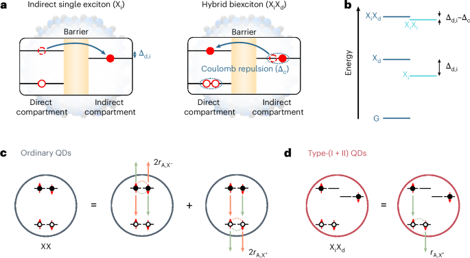
CdSe (r = 2.6 nm)/Cd1−xZnxSe (l = 1.7 nm)/CdS (h = 2.2 nm)/ZnS (d = 0.3 nm) type-(I + II) QDs were synthesized following the procedure described previously23,24. In a typical synthesis, 0.1 mmol of cadmium oleate and 6 ml of ODE were loaded into a reaction flask, degassed at 110 °C and purged with nitrogen. After heating to 310 °C, 0.2 mmol of TOPSe was injected, followed by a gradual addition of 1 ml of TOP, forming CdSe cores with a radius of 1.5 nm. The core radius was then increased to 2.6 nm by adding 0.25 mmol of cadmium oleate and 0.25 mmol of TOPSe. To form a compositionally graded Cd1−xZnxSe layer, 0.4 mmol of zinc oleate, 0.19 mmol of cadmium oleate and 0.38 mmol of TOPSe were injected at 310 °C, followed by a second injection of 1.31 mmol of zinc oleate and 1.52 mmol of TOPSe. After a 30 min reaction, the Cd1−xZnxSe barrier layer was complete. For the CdS layer, 4 mmol of OT and cadmium oleate were added stepwise. The ZnS shell was grown by injecting 2 mmol of OT and 4 mmol of zinc oleate, followed by an additional 2 mmol of zinc oleate after 30 min. After cooling, the QDs were purified and redispersed in toluene for further use.
Synthesis of ccg-QDs
The synthesis of compact compositionally graded ccg-QDs with the CdSe/Cd1-xZnxSe/ZnSe1-ySy structure (rCdSe = 2.6 nm, lCdZnSe = 2.7 nm, dZnSeS = 1.7 nm, and x and y vary from 0 to 1 in the radial direction towards QD periphery) follows the procedure described previously31,37, with minor modifications. The CdSe core with a radius of 2.6 nm was prepared using the same method as for the type-(I + II) QDs. To grow the compositionally graded Cd1-xZnxSe layer on top of the CdSe core, a mixture of 0.75 mmol of cadmium oleate and 2.5 mmol of TOPSe was slowly injected into the reaction flask over 40 min, accompanied by a stepwise injection of zinc oleate (total 5 mmol). For the growth of the compositionally graded ZnSe1-ySy layer, 5 mmol of zinc oleate was first added, followed by the dropwise injection of 2.5 mmol of TOPSe over 1 h. During this step, 0.25 mmol, 0.5 mmol and 0.75 mmol of TOPS were injected at 15 min, 30 min and 45 min, respectively. Finally, 1 mmol of TOPS and an equivalent amount of zinc oleate were injected, and the reaction was allowed to proceed for an additional 30 min.
Synthesis of g-QDs
The following procedure was used to prepare quasi-type-II thick-shell g-QDs with the CdSe/CdS/ZnS structure (rCdSe = 2.6 nm, hCdS = 3.2 nm, dZnS = 0.3 nm). The CdSe core, with a radius of 2.6 nm, was synthesized using the same method as for the type-(I + II) QDs. Before growing the CdS layer, 3 ml of oleylamine was injected into the flask, and the reaction temperature was lowered to 270 °C. Over the next 3 h, 2.8 mmol of OT was slowly injected along with a stepwise addition of 1.2 equivalents of cadmium oleate. After the CdS layer growth, the temperature was raised to 300 °C, and the outer ZnS layer was formed by adding 1.5 mmol of OT and 3 mmol of zinc oleate.
Synthesis of thin-shell CdSe/ZnS QDs
CdSe/ZnS QDs with rCdSe = 2.5 nm and dZnS = 0.5 nm were synthesized as follows. A mixture of 1 mmol of CdO, 700 mg of MA and 15 ml of ODE was added to a reaction flask and degassed under vacuum. The flask was then back-filled with nitrogen and heated to 270 °C, maintaining this temperature for 30 min to achieve a clear solution. TOPSe (0.5 mmol) was injected to form CdSe cores with a radius of 2.5 nm. To grow the ZnS shell, 2 mmol of zinc oleate and 1.5 ml of DDT were injected into the flask, and the temperature was raised to 300 °C. After 30 min, 2 mmol of OT and 2 mmol of zinc oleate were added, and the reaction continued for an additional hour.
ASE measurements
The QD film samples were prepared on a glass substrate using a multi-step coating and crosslinking process with 1,8-diaminooctane as a linking agent32. The film thickness was ~300 nm. The substrate was attached to a copper holder acting as a heat sink. The sample assembly was mounted on the cold finger of a cryostat (Janis Research, VPF-100) and cooled with liquid nitrogen during ASE measurements.
The QD sample was excited using the second harmonic of a Q-switched Nd:YLF laser (Spectra-Physics, Empower), with a photon energy of 2.4 eV and a pulse duration of 230 ns (FWHM). The laser repetition rate was reduced from 1,000 Hz to 250 Hz using a chopper.
The laser beam was focused into a thin stripe (100 µm × 4 mm) on the QD film using a cylindrical lens. The stripe was aligned approximately perpendicular to the sample’s edge and positioned to be partially truncated by it. Emission from the sample’s edge was collected along the excited stripe’s direction. The collected light was then spectrally dispersed using a Czerny-Turner spectrograph (Acton 500i) and analysed with a nitrogen-cooled charge-coupled device (CCD) camera (Roper Scientific).
Fabrication of a DFB laser
The one-dimensional SiO2-DFB grating was fabricated on a glass substrate using laser interferometric lithography. The grating period (ΛDFB) was 345–355 nm. The groove height was 50 nm, and the groove width was 0.7ΛDFB.
The glass substrate was cleaned via sonication in acetone and isopropyl alcohol. A 50-nm-thick SiO2 layer was then deposited using electron beam evaporation. The anti-reflection coating (ARC), i-CON-16, was spin-coated at 3,000 rpm for 30 s, forming a 150-nm-thick film, which was subsequently annealed at 190 °C for 1 min.
A 500-nm-thick negative photoresist (NR7-500P, Futurex) was spin-coated on the ARC under the same conditions (3,000 rpm for 30 s) and annealed at 150 °C for 1 min. The photoresist was then exposed to a 355 nm laser at a 90 mJ dose for 11.4 s using an interferometric lithography system. After exposure, the sample was annealed at 100 °C for 1 min and developed in RD6 (Futurex) for 40 s.
Inductively coupled plasma (ICP) etching was performed to remove the ARC, SiO2 and photoresist layers, using the following gas flows: O2 (30 sccm) for photoresist etching; CHF3 (45 sccm) + O2 (5 sccm) for SiO2 etching; and O2 (30 sccm) for ARC etching.
Characterization of a QD-DFB laser under cw excitation
The fabricated QD-DFB laser was placed inside a cryostat (Janis Research, VPF-100). It was excited at 2.8 eV using a laser diode (Opt Lasers, PLH3D). The pump laser output was electrically modulated to generate pulses with durations ranging from 1 μs to 10 μs (FWHM) and repetition rates between 0.1 kHz and 10 kHz. The pump beam was focused onto the sample, forming a spot measuring 150 µm by 400 µm. The light emitted from the surface of the QD-DFB laser was spectrally dispersed using a Czerny-Turner spectrograph (Acton 500i) and analysed with a nitrogen-cooled CCD camera (Roper Scientific).
Fabrication of EL-active lasing devices
The fabrication of EL-active lasing devices begins with the preparation of a SiO2-DFB grating on a glass substrate coated with ITO. The fabrication process follows a procedure similar to that used for SiO2-DFB/glass devices described earlier (see above).
Fabrication of optically excited devices
For devices intended for optical excitation measurements, the DFB/ITO/glass substrate was cleaned by sonication in isopropyl alcohol. A 50-nm-thick ZnO electron transport layer was deposited using the sol–gel method and annealed at 200 °C for 1 h. A densely packed QD film was formed using a multi-step coating and crosslinking process32. Each layer was spun at 2,000 rpm from a QD solution in n-octane (50 mg ml−1), resulting in a total QD layer thickness of 150 nm. The QD layer was annealed at 100 °C for 10 min.
Next, a 50-nm-thick HTL of poly(9,9-dioctylfluorene-alt-N-(4-sec-butylphenyl)-diphenylamine) (TFB) was deposited by spin-casting at 4,000 rpm for 20 min. A 50-nm-thick HIL of dipyrazino[2,3-f:2′,3′-h]quinoxaline-2,3,6,7,10,11-hexacarbonitrile (HAT-CN) was then deposited using thermal evaporation. Finally, the device was completed with the deposition (also via thermal evaporation) of a 100-nm-thick Ag layer, serving as the anode.
Fabrication of electrically excited devices
Devices intended for EL measurements included an additional dielectric interlayer of LiF, with a current-focusing aperture prepared as a 50-µm-wide slit. This interlayer was inserted between the HTL and HIL and deposited using thermal evaporation. The slit was defined using a shadow mask. To further enhance the current-focusing effect, the top Ag contact was patterned as a narrow 300-µm-wide strip, orthogonal to the slit in the LiF layer.
Electrical characterization of EL devices
The current density—voltage (j–V) characteristics of the devices were measured using square voltage pulses generated by a function generator (Tektronix AFG320) and amplified by a high-speed bipolar amplifier (HSA4101, NF Corporation). The voltage across the device was monitored using a Tektronix TDS2024B oscilloscope, connected to the amplifier’s monitoring port. The transient current was determined by measuring the voltage drop across a 10 Ω load resistor placed in the return path.
Fabrication of QD microdisk lasers
QD microdisk lasers were fabricated using photolithography and plasma etching techniques. First, a 200-nm-thick QD film was deposited onto a glass substrate through a multi-step coating and crosslinking process32.
For photolithography, AZ5214E photoresist was spin-coated onto the QD film at 4,000 rpm for 30 s, followed by baking at 100 °C for 5 min. The photoresist was then ultraviolet-exposed, developed using AZ 400 K developer and rinsed with deionized water. The remaining photoresist acted as a soft mask for the subsequent inductively coupled plasma-reactive ion etching (ICP-RIE) process. During ICP-RIE etching, a gas mixture of 18 sccm H2 and 7 sccm Ar was used under 50 W radio-frequency power and 200 W ICP power. This process yielded an etch rate of 300 nm min−1, producing smooth-sided microdisks. Finally, the photoresist was removed from the QD microdisks using acetone.
Characterization of QD lasers using short-pulse pumping
The EL-active and microdisk QD lasers were characterized using excitation by 190 fs, 2.4 eV second-harmonic pulses generated by a regeneratively amplified Yb:KGW femtosecond laser (Pharos, Light Conversion) equipped with a HIRO harmonic generation module (Light Conversion).
The QD-based devices were placed at the focal plane of the collecting lens. The emitted light was spectrally dispersed using a Czerny-Turner spectrograph (Acton Research 500i) and analysed with a nitrogen-cooled CCD camera (Roper Scientific).