
Tom’s Hardware Premium Roadmaps
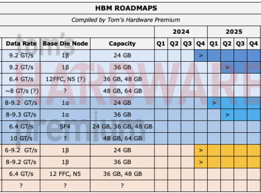
(Image credit: Future)
As AI accelerators and HPC devices grow larger and more complex, advanced chip design continues to move away from the transistor and toward the package. Over the past year, packaging engineers and foundries have converged on the same conclusion — that 2.5D integration is now the primary tech responsible for power delivery, signal integrity at extreme bandwidths, mechanical stability across large areas, and in some cases, even active functionality.
That is apparent across the industry, from thicker silicon interposers designed to support HBM4, to renewed interest in silicon bridges and longer-term interest in organic and glass alternatives. The technology itself is not new, but it’s facing all-new constraints as AI has pushed 2.5D packaging into territory where its original cost and yield assumptions no longer hold, and the next phase is about deciding which problems are worth solving in silicon and which are not.
Interposers are becoming power platforms
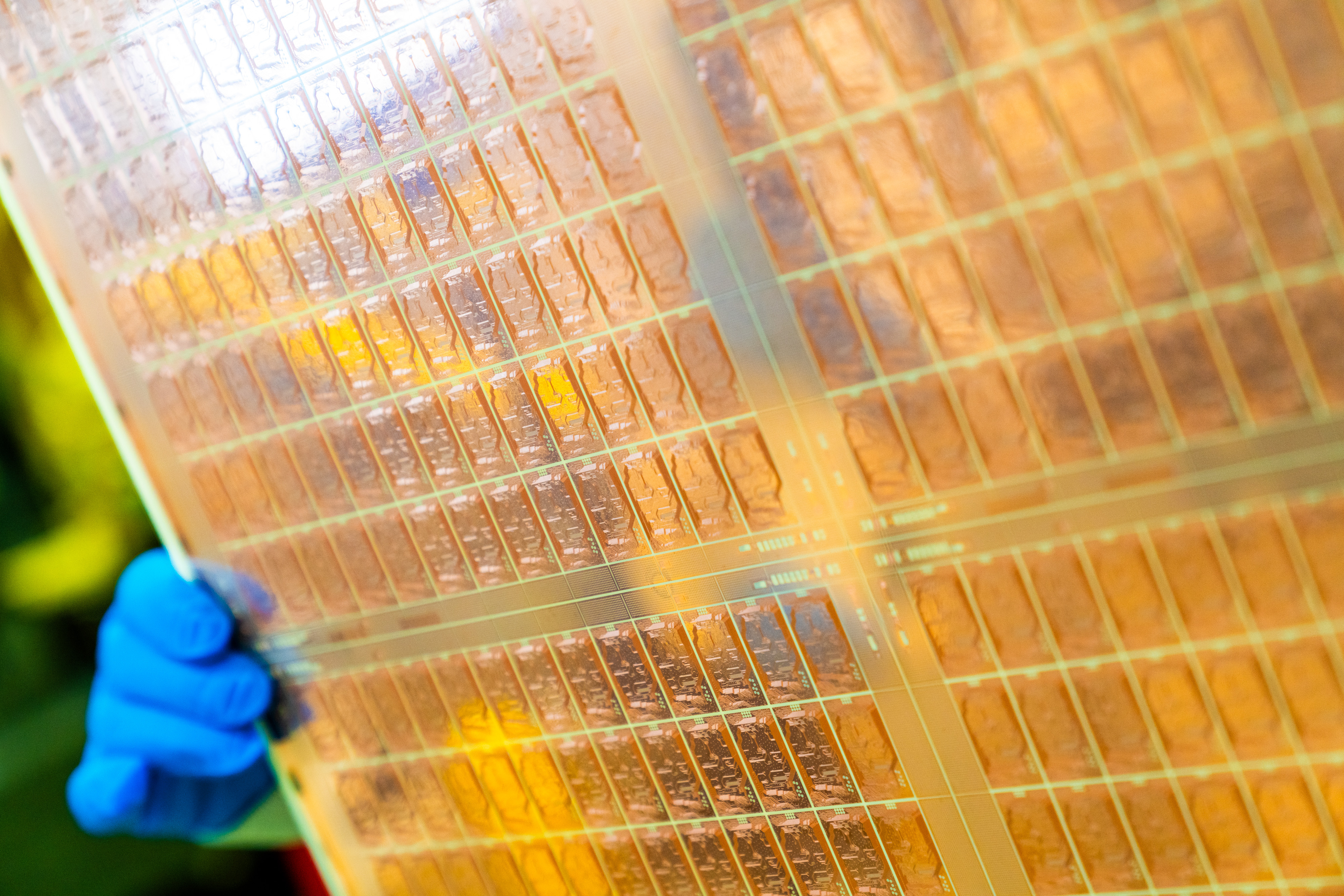
One of the more immediate trends in 2.5D packaging is the steady thickening and layering of silicon interposers. Early interposers were largely routing fabrics, optimized to move signals between logic dies and the adjacent memory stack, but that role has since grown. As memory interfaces widen and chiplet counts increase, the interposer is expected to carry far more current and maintain signal integrity across much denser wiring.
You may like
Vendors now routinely talk about moving beyond four metal layers. Designs targeting post-HBM3 systems are already planning for eight or nine layers — or sixteen — driven by a combination of routing density and power distribution needs. Each additional layer increases fabrication cost, but the more pressing issue is mechanical. Thick, multilayer interposers are prone to warpage, and controlling flatness across a larger area has become a concern.
(Image credit: TSMC)
This has given rise to something of a balancing act. Thinner interposers reduce signal path lengths and can improve electrical performance, but they are mechanically fragile. Thicker interposers offer more routing headroom and stiffness, but increase stress and thermal complexity. Engineers are leaning on workarounds like thin-film stress control and tighter process windows to keep large interposers flat enough for assembly, but margins are narrowing as sizes increase.
The logical extension of this trend is the active interposer. Once the interposer carries significant power and routing infrastructure, the temptation to integrate logic grows. However, active interposers remain rare because they fundamentally change the yield model. A passive interposer can be treated as a mechanical and wiring component, but an active one must be tested as a functional die, introducing new failure modes and validation steps.
This means active interposers are largely confined to high-value AI and HPC designs where the system-level benefits outweigh potential yield penalties.
Some vendors are already blurring the line. Certain advanced packages use base dies that look like interposers, but include active circuitry for data movement and memory control. These designs shift complexity downward in the stack, reducing the burden on the top-level compute dies while concentrating risk in fewer large silicon components. The approach works, but it reinforces the idea that the interposer is becoming part of the overarching architecture.
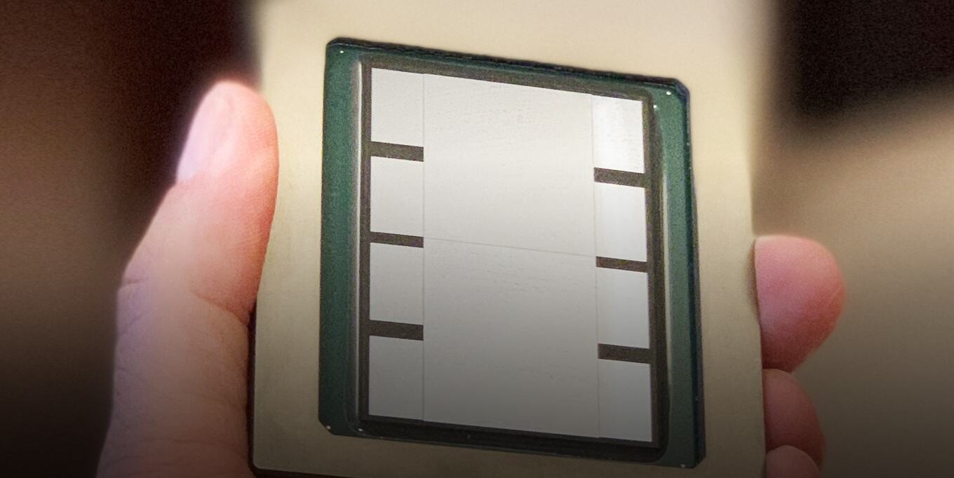
Silicon bridges still promise savings
(Image credit: Intel)
If interposers are becoming more expensive and complex, silicon bridges are supposed to provide some relief by replacing a large silicon interposer with small, high-density bridge dies embedded in an organic substrate. As is predictably the case, there is a limiting factor here – assembly yield.
The challenge is not fabricating the bridges themselves, which are small and yield well, but aligning multiple chiplets across those bridges with sufficient accuracy. Placement offsets between dies are unavoidable at scale, and these offsets can break finely patterned interconnects that rely on ideal alignment.
You may like
That has given rise to a paradox of sorts. Bridges promise lower silicon cost, but misalignment during assembly can push overall yields low enough that the package becomes more expensive than a traditional silicon interposer solution. Some companies are experimenting with adaptive patterning techniques that compensate for placement offsets by modifying interconnect layouts after die placement. These methods can recover yield, but they introduce throughput penalties because patterning becomes die-specific.
You could relax design rules by using larger interconnect features, which can tolerate more misalignment, but that erodes the density advantage that justified using silicon bridges in the first place. Ultimately, there’s a narrow operating window where bridges deliver both acceptable yield and meaningful cost savings. Bridges continue to improve, and incremental gains in placement accuracy and adaptive processing may eventually unlock their potential, but they are not yet a universal substitute.
Silicon still anchors HBM
The longer-term effort to reduce 2.5D packaging cost concerns alternative materials, with organic interposers being a promising candidate. They can be built using panel-level processes, avoid expensive silicon steps like TSV formation, and scale more naturally with substrate manufacturing infrastructure.
Again, there’s a challenge: density. Traditional package substrates operate at line and space dimensions that are an order of magnitude coarser than silicon interposers. Pushing organic interposers down to five microns requires cleanroom environments and tighter process control, narrowing the cost gap with silicon. Advanced materials like Ajinomoto build-up films help, but they raise material costs even as they improve performance.
High-bandwidth memory (HBM) is only complicating matters because, as memory interfaces tighten and stack counts increase, pad pitches shrink. Silicon handles this comfortably, but organic materials do not, at least not yet. Research efforts are underway to integrate HBM on organic interposers, but these remain experimental. For the highest bandwidth designs, silicon continues to be the default because it offers predictable pitch control and proven reliability.
Organic interposers are expected to coexist with silicon rather than replace it outright. Where bandwidth and density demands allow, organic solutions can reduce cost and improve scalability. Where they do not, silicon remains unavoidable.
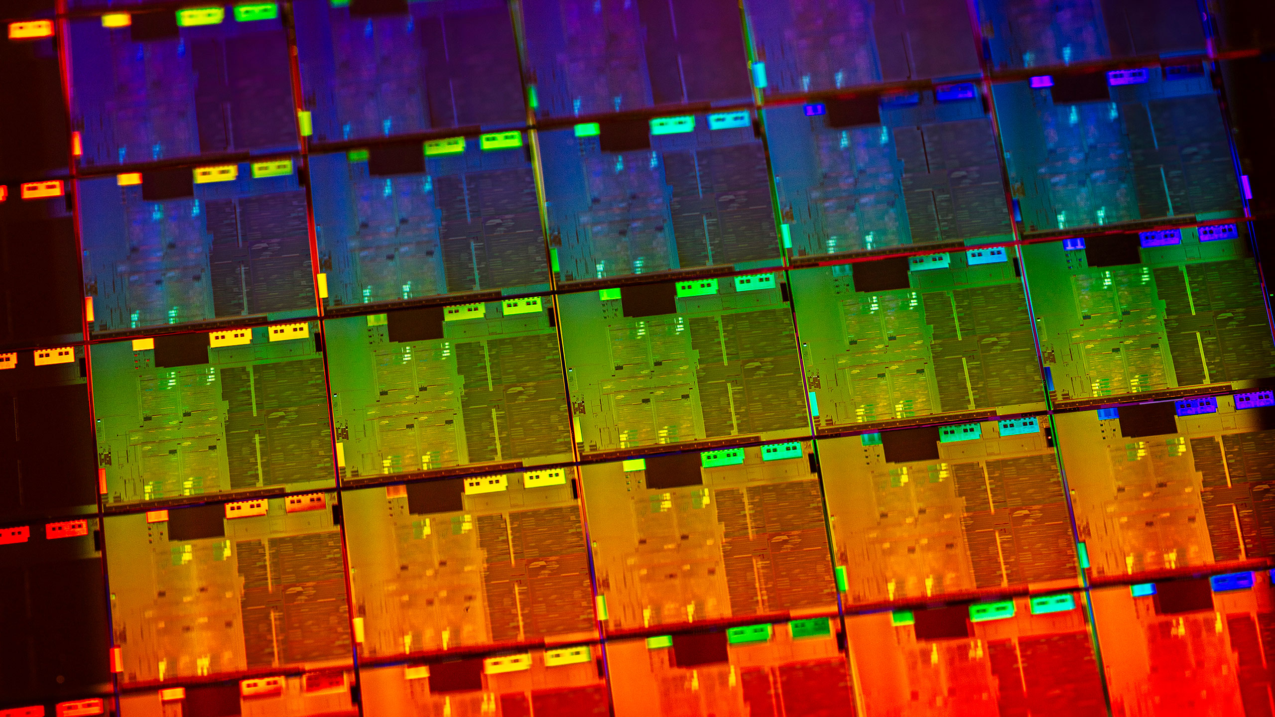
(Image credit: Intel)
Glass interposers are potentially the next step beyond organic. These offer excellent electrical properties, low thermal expansion, and compatibility with large panel formats. They also open interesting possibilities for optical integration. However, glass cannot host active circuitry, and the ecosystem required to process and standardize glass substrates at scale is still forming.
With glass interposers, we’re generally looking towards 2030 in terms of volume production. Pilot lines have emerged, but widespread adoption will naturally depend on factors such as tooling and supply chain maturity. In the near-term, if anywhere, they are likely to appear in niche applications rather than a drop-in for silicon.
What’s most apparent is that 2.5D is fragmented, with no single, viable pathway toward cheaper, simple packaging – at least not yet. Instead, AI demand is pushing silicon interposers to become thicker and more layered, with bridges continuing to chase cost advantages but remaining constrained by assembly. Organic and glass could be promising alternatives, but only within specific applications.