
The studied samples consist of rectilinear bars carved by FIB machining from a bismuth single crystal (Fig. 2). The details of the fabrication, particularly the great care taken to avoid any residual thermal mismatch strain by membrane suspending the bismuth structures, are detailed in Methods. As FIB machining is a maskless, direct-write technique, such structures can be modified sequentially and the effect of the modifications is probed one by one. Here individual grooves of approximately 0.3 μm × 0.3 μm cross-section are added to the device to iteratively track the transport response to such surface modifications. Without magnetic fields, the conduction of our devices is mainly governed by the bulk conductance, as expected. The temperature-dependent resistivity ρ(T) agrees well with measurements on the bulk bismuth crystal, with excess scattering from finite-size effects (Supplementary Note 1). The comparatively low residual resistivity ratio of the parent crystal of around ρ(300 K)/ρ(2 K) ≈ 27 indicates a moderate crystalline quality of bismuth, which was chosen on purpose to reduce classical finite-size effects and bulk conduction, to focus on the influence of the surface on transport. Measurements with an increasing number of grooves along the channel up to N = 7 are overlaid, and barely any differences are notable over the entire range of temperatures (T = 2–300 K; Fig. 2c). This is not surprising given the minute modification amounting to a total loss of 2% of the material. On closer inspection, the conductance of the device with N grooves, GN, decreases as a function of N up to 2% (Fig. 2c, inset), which matches the loss of material and, therefore, agrees with the expectation of removing bulk channels. These results are entirely compatible with dominant bulk conduction in a device at zero field, as expected for a semimetal.
Fig. 2: Seeding chiral boundary states via FIB-cut grooves.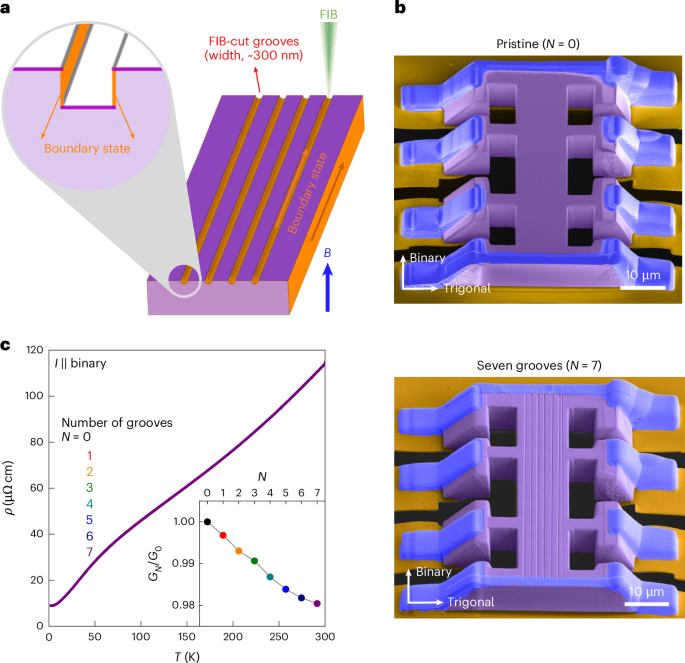
a, Schematic of chiral boundary states in a microstructured bismuth with FIB-cut grooves. Under strong magnetic fields driving the system into the quantum limit, bulk states are quantized, and chiral boundary states along the side surfaces parallel to the magnetic field dominate the charge conduction of the cuboid bismuth microstructure. By cutting grooves on the top surface with FIB, additional conduction paths are formed along the sidewalls of FIB-cut grooves. b, Scanning electron microscopy images of a microstructured bismuth before (top) and after (bottom) cutting seven grooves. c, Temperature-dependent electrical resistivity ρ(T) of the microstructured bismuth with increasing number of grooves N on its surface. The inset shows the conductance of N-groove state GN normalized by that of the pristine state G0 at T = 2 K.
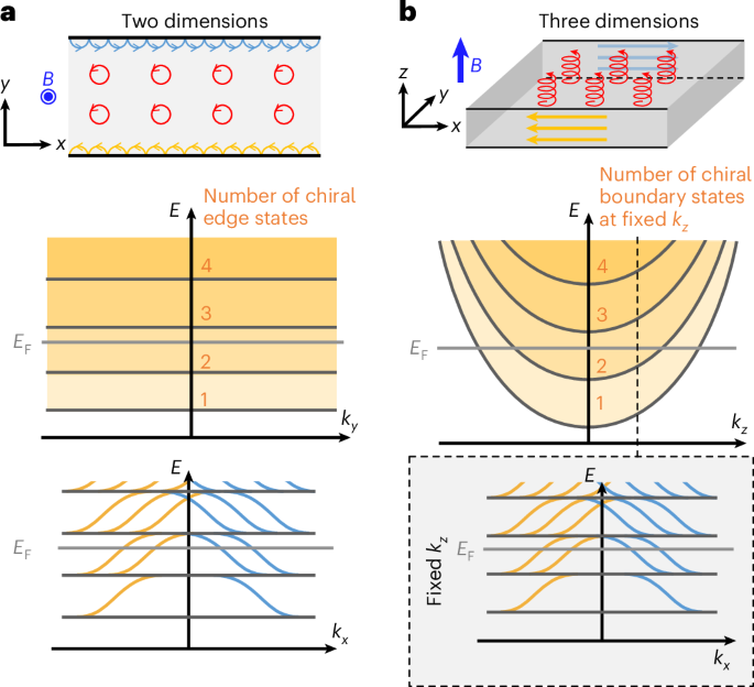
Next, out-of-plane magnetic fields are applied to drive the material into the quantum limit and probe the evolution of conduction (Fig. 3). The magnetoresistance (MR) R(B) is quadratic in B around zero field followed by strong, B-linear growth, which abruptly terminates at a clear kink at B* ≈ 2.7 T, above which a saturated, sublinear behaviour is observed (Supplementary Fig. 2). This field scale coincides with the quantum limit BQL ≈ 2.5 T of electron pockets at the L points in this field direction21 obtained self-consistently from quantum oscillations (Supplementary Note 2). Although the bulk crystal and microsample behave similarly in the low-field regime, they strongly differ in the quantum limit: the MR in the bulk crystal continues to grow without anomalies, as expected for the well-known nearly compensated semimetal behaviour of bismuth (Supplementary Fig. 1)21,26. A simple bulk band picture (for example, a two-band model) cannot account for this behaviour over the entire field range (Supplementary Note 3). Therefore, this observation points to the sizable surface conduction in the quantum limit, which naturally is more dominant in the microscopic bar. The link to the quantum limit strongly suggests that chiral boundary states play an important role, a connection that can be further substantiated by experiments.
Fig. 3: Magnetotransport of FIB-cut grooves.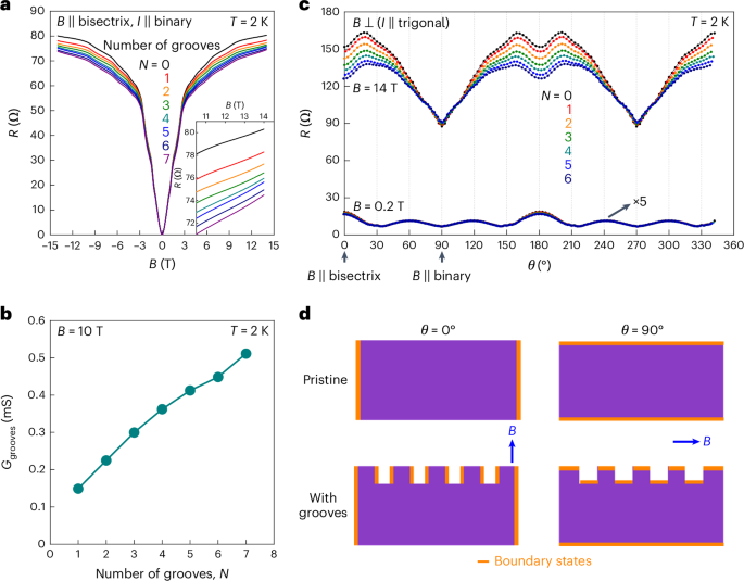
a, Magnetic-field-dependent electrical resistance R(B) of the N-groove state with B ∥ bisectrix and I ∥ binary at T = 2 K. The inset shows R(B) in high magnetic fields (B > 10 T). b, Conductance of grooves Ggrooves as a function of N with a magnetic field of 10 T at 2 K. The parallel-conductor model is used in estimating Ggrooves (Methods). c, Angle-dependent electrical resistance R(θ) of the N-groove state, where the magnetic field B (0.2 T, 14 T) is rotating in the plane perpendicular to the current direction (I ∥ trigonal) at T = 2 K. d, Schematic of the chiral boundary states in the microstructured bismuth with different field angles. When the system is in the quantum limit, chiral boundary states (highlighted with the orange area) along sidewalls parallel to the magnetic field dominate the surface conduction. Cutting grooves effectively increases the surface area of the chiral boundary states under the out-of-plane magnetic field (θ = 0°) but make negligible change with the in-plane magnetic fields (θ = 90°).
The evolution of MR when adding grooves provides such a test for surface conduction. Indeed, the MR monotonically decreases as a function of N, which is prominent in high magnetic fields above B* (Fig. 3a). For example, at B = 14 T, the resistance decreases from R ≈ 80 Ω of the pristine (N = 0) sample to R ≈ 74 Ω of the seven-groove (N = 7) sample, a reduction of approximately 7.5% (Fig. 3a, inset). Such a stronger effect of the grooves is opposite to the zero-field behaviour, as adding grooves increases the conductance above the quantum limit despite the reduction in the cross-sectional area (Fig. 3b). All these experiments are well reproduced in four bismuth microstructures despite a distinct variance in the groove depth and width (Supplementary Note 4), strengthening the evidence for conduction channels along the grooves. The additional surface conduction along the grooves reduces current flowing through the bulk, thereby consistently decreasing the Hall voltage of the device (Supplementary Fig. 5). As the grooves are connected between the current contacts bypassing the voltage contacts, they have an indirect and subdominant effect on the Hall voltage compared with the sidewalls of a rectilinear bar (Supplementary Note 5). We note that this experiment has no analogy in two dimensions as the number of edge modes in a 2D system is given by the Landau level index alone, regardless of the sample geometry. Thus, it is impossible to address the debate about whether currents run on the edge or in the bulk in the 2D QHE by similar geometric sample designs1.
A further test of the chiral surface states involves the MR dependence on the field angle (Fig. 3c,d). It is yet another unique feature of 3D mesostructures in the quantum limit, as 2D QHE is purely driven by orbital effects that only depend on the scalar projection of the magnetic field onto the plane. In three dimensions, the field direction’s role is much richer as it sets the quantization direction for the Landau levels with respect to the surfaces. At low fields below the quantum limit (B = 0.2 T), the angle-dependent MR R(θ) of the bars shows a 60° periodicity, reflecting the three-fold rotational symmetry of the crystal lattice and the bulk electronic system (with a weak two-fold component from classical ballistics; Supplementary Note 2)27,28,29. On the other hand, R(θ) in the quantum limit (B = 14 T) exhibits a strong two-fold symmetric response, which clearly reflects the sample shape instead of the lattice symmetry. The minimal value of the resistance is found for fields parallel to the long sideface of the bar (θ = 90°), which corresponds to the larger surface of the rectangular bars. A shallower local minimum replaces the maximum MR in low fields at θ = 0°, when the field is along the short face. We conclude that the excess conductivity is not an intrinsic property of the bar, but selectively arises in those sidewalls parallel to the magnetic field, which is where the chiral edge currents are located.
This point is further strengthened when the grooved samples are considered. The grooves cause a substantial difference in the angle-dependent MR. Under an out-of-plane magnetic field of 14 T (θ = 0°), MR of the device with N = 6 grooves decreases almost 15% from the pristine state, in stark contrast to the negligible change observed at θ = 90°. An explanation is found when considering the projected surface area. Although for θ = 0°, the effective sidewall area is increased by the grooves, their net effect on the surface area for θ = 90° is zero (Fig. 3d). The field selectivity of the conductive surface further speaks against inadvertent surface modifications from FIB fabrication. Indeed, Xe-based machining of an elemental metal yields high-quality surfaces without compositional disorder and a sharply terminated single-crystal surface covered by few nanometres of nanocrystallite bismuth (Supplementary Note 6 provides an in-depth surface analysis via scanning transmission electron microscopy). The intrinsic nature of the chiral edge conductance in the quantum limit further reflects in reports of parallel-field-enhanced transport in macroscopic bismuth single crystals on the millimetre scale, where a substantial contribution of surface currents to the transport depends on the shape of the crystal29.
The experimental observations unequivocally demonstrate substantial charge transport carried by chiral edge currents, which naturally arise from microscopic modelling in tight-binding calculations (Methods). The calculated Landau band structure of bismuth captures the experimental situation with the electron pockets at the L points from three valleys being in the quantum limit, and a hole pocket at the T point that is not (Fig. 4a). Here the occupied momentum range of kz at the lowest Landau band contributes to chiral boundary states, which is highlighted in the (side) surface spectral function (Fig. 4b). In this picture, the number of surface modes contributing to transport should scale with the groove depth, though the effect of hybridization between modes and confinement for shallow grooves (less than 300 nm deep) may lead to small modifications from a linear relation. The linear relation is indeed confirmed by varying the depth of the grooves within the same device and estimating the conductance of each groove, denoted as Ggroove (Fig. 4c and Supplementary Note 4).
Fig. 4: Non-local magnetotransport of FIB-cut grooves.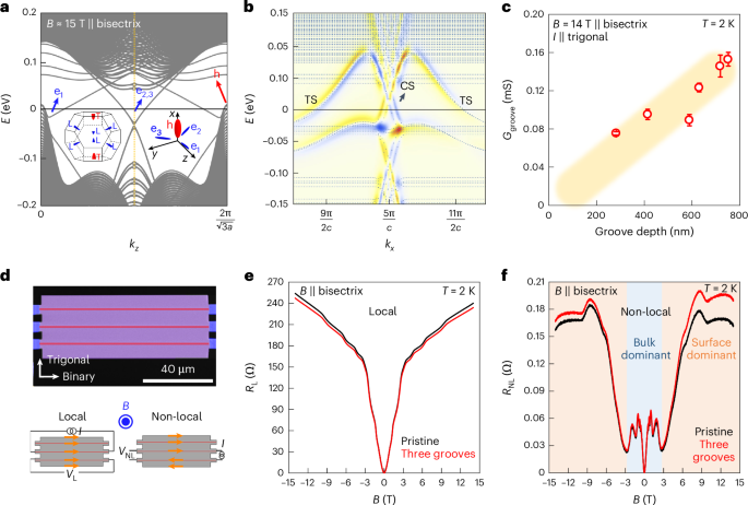
a, Landau band structure of bismuth when a magnetic field B ≈ 15 T is applied along the bisectrix axis (Ny = 1,500). The magnetic field is strong enough for all electron pockets at the L point from different valleys (e1–e3) to be in the quantum limit, except the hole pocket (h) at the T point. The dashed orange line indicates the kz momentum for the surface spectral density in b. The insets depict the sketch of the Brillouin zone and Fermi surfaces of bismuth. b, Surface spectral density for B ≈ 15 T for a slab thickness of Ny = 1,500 unit cells. The localized states on opposite sidewalls are differentiated by yellow and blue. The chiral surface states (CS) manifest an imbalance between right- and left-moving modes on each surface, whereas the trivial surface states (TS) come in pairs of right and left movers per surface. c, Conductance of individual groove Ggroove as a function of groove depth, with B = 14 T along the bisectrix at T = 2 K. The error bars represent the variation obtained by averaging two longitudinal voltage pairs of the Hall-bar structure. d, Scanning electron microscopy image of a non-local geometry device, after cutting three grooves (red lines) between each longitudinal electrodes pair (top). Bottom: schematics of the local (left) and non-local configurations (right) of current and voltage electrodes. The effective current paths via chiral boundary states in the device are highlighted as arrows. e,f, Magnetic-field-dependent local resistance RL (e) and non-local RNL (f) at T = 2 K, where RL(NL) = VL(NL)/I, before (black) and after (red) cutting three grooves.
A different possible origin of the excess conductance observed in our experiments may be regular surface states, especially well known to be metallic and abundant in bismuth30. Indeed, our calculations consistently yield surface states corresponding to large Fermi surfaces (Supplementary Fig. 7). However, they are difficult to reconcile with an enhancement in sidewall conductivity that follows the direction of the magnetic field. The size of the Fermi surface implies that the surface is far from the quantum limit under laboratory fields; hence, a semiclassical description is applicable. In this surface-state scenario, the semiclassical surface may either be in a clean limit ωcτ ≫ 1 or dirty limit ωcτ ≪ 1 (ωc is the cyclotron frequency and τ is the relaxation time). Within the diffusion picture of the dirty limit, magnetic fields have a negligible effect on transport from a Kohler scaling argument, contrary to the experimental observation. This leaves only a surface state in the clean limit, in which the magnetic field ought to completely suppress the conductance in surfaces normal to the field. Hence, carriers in perpendicular fields would be localized, whereas sidewalls under parallel fields remain highly conductive due to the lack of orbital effects. This scenario is also at odds with our observations. First, the zero-field resistivity increases when adding grooves, despite the growing surface-to-bulk ratio. Further, these surface states do not appear as Shubnikov–de Haas oscillations despite the need for them to be in the clean limit. Last, a clean-limit surface is difficult to reconcile with the nanocrystalline, disordered nature of the FIB-irradiated surface. In particular, naturally introduced nanometric roughness on the sidewall, due to ion-beam interactions that depend on the crystallographic orientation of bismuth (Supplementary Note 7), should strongly suppress conduction via trivial surface states; however, our observation shows that surface conduction remains robust against such roughness. This is consistent with the chiral-boundary-state scenario, as they remain unimpeded by such surface disorder akin to the robust nature of the 2D QHE edges.
A further direct test for chiral boundary states is the strong non-locality of transport emerging in the quantum limit. In quantum Hall states, quantum spin Hall states and topological insulators, non-locality has been a key observable to demonstrate their non-trivial charge flow31,32,33,34,35,36. To this end, we probe a rectangular microstructure with six electrodes, three close-by ones on each side (5-μm spacing) separated by a 96-μm-long block of bismuth (Fig. 4d). In this geometry, we can first probe the local resistance RL = VL/I, which arises from currents flowing across the whole microstructure. This can be compared with the non-local resistance RNL = VNL/I, where currents flow within one side of the microstructure and non-local signals are received between voltage electrodes on the opposite side. The ohmic contribution to the non-local voltages at distance L given the local spacing of electrodes w is suppressed by a factor exp(–πL/w) when L ≫ w (refs. 36,37). The zero-field voltage measured in the non-local configuration is consistently observed to be reduced by a factor of 100 compared with the local current configuration (RNL ≈ 0.01RL). Connecting these far-away electrodes by grooves should enhance non-locality and increase the far-away voltage signals above the ohmic limit given they host chiral conductive states. This is indeed observed experimentally.
At zero field, no change to the non-local signal from added grooves is observed, as expected from the negligible change in shape, further excluding the addition of a trivial conductive layer. Below the quantum limit, RNL(B) exhibits substantially enhanced quantum oscillations, reflecting the sensitivity of charge injection to Landau quantization. As the material enters the quantum limit, RNL(B) steeply rises. In particular, this rise begins only beyond the kink of the local MR at B* ≈ 2.7 T. Evidently, the current distribution substantially changes in the quantum limit, and the sublinearity of RNL(B) in high fields is associated with substantial surface currents. Although RL(B) increases by 32% from 6 T to 14 T, RNL(B) remains at a saturated value in the high-field region. Such behaviour is naturally expected from chiral boundary states, which, once formed in the quantum limit, exhibit no further field dependence.