
Characterizations of ferroelectricity in WTe2
WTe2 exhibits various crystal structures, such as 2H, 1T’, and Td. In the Td phase (Td-WTe2, space group Pnm21), the tungsten (W) atoms are surrounded by octahedra formed by the tellurium (Te) atoms. Due to strong metallic bonding interactions, the W atoms form slightly bent zigzag chains, leading to distortions in the Te octahedra12 (Fig. 1a). Spontaneous polarization appears in the Td phase with a 1T’–Td phase transition temperature of 565K25. The structure possesses a a-c mirror plane (Fig. S1b), which constrains the polarization to be parallel to the a-c plane. Under an external electric field, the out-of-plane polarization component can be reversed through relative displacements of the neighboring layers11. In Fig. 1a, the direction of interlayer displacement during polarization reversal is indicated by the reddish-brown arrows, while the red arrow denotes the out-of-plane polarization direction.
Fig. 1: Device structure and ferroelectric characterizations.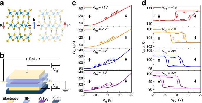
a Crystal structure of Td-WTe2 in different polarization states. The red arrows indicate the polarization direction, while the reddish-brown arrow represents the sliding direction. W and Te atoms are represented by blue and yellow spheres, respectively. b Schematic diagram of the BN/WTe2/BN dual-gate device. Vtg and Vbg are applied to the top and bottom BN layers, respectively, while the conductance of WTe2 is measured through in-plane electrodes. c, d In-plane conductance of WTe2 under different bottom gate voltages, with measurements taken under continuous Vt and after applying the pulse Vtg-p. Colored arrows indicate the evolution of in-plane conductance with varying Vtg, while black arrows denote the polarization direction.
WTe2 single crystals were synthesized using the CVT method (See “Methods” for details) and their structures confirmed by Raman spectroscopy (Fig S1c), which is consistent with previous reports26. Due to the semimetallic nature of WTe2, applying an electric field directly to the material poses challenges. To address this issue, we employed the BN/WTe2/BN dual-gate device structure (Fig. 1b, optical image of Device 1 shown in Fig. S5a). It allows for an effective application of the electric field to the conductive material and is widely used in measurements of sliding ferroelectrics9,11,13. To align with subsequent switching kinetics measurements, we employed one of the gates to induce polarization reversal in the material by scanning the voltage in both positive and negative directions, while keeping the voltage on the other gate constant. During the voltage scan, we measured the in-plane conductance of WTe2 using the in-plane electrodes located underneath the WTe2, as illustrated in Fig. 1b. In Fig. 1c, we show the typical results of such a device measured at 100 K. Under a given bottom gate voltage (Vbg), the in-plane conductance (Gon) measured under continuous top gate voltage (Vtg) scan exhibits a characteristic “butterfly” shape (Fig. 1c). By changing the Vbg, we can shift the butterfly loop horizontally. Though reported frequently as an indication of ferroelectricity in vdW ferroelectric materials, the exact mechanism of the butterfly loop has not been discussed in the literature. We suggest that this phenomenon arises from the combined effect of the polarization-induced asymmetric distribution of intrinsic carriers in WTe227 and the preferential doping of external carriers into the WTe2 layer closest to the gate dielectric28. The in-plane conductance of WTe2 exhibits a polarization-dependent shift in its response to gate voltage, ultimately resulting in a characteristic butterfly-shaped curve (Fig. S3, see SI section 2 for detailed analysis).
To better demonstrate the ferroelectric behavior of Td-WTe2, we conducted static pulse switching measurements (Fig. S4). In this case, the Vtg was applied in pulses (denoted Vtg-p). After each pulse, the in-plane conductance was measured while the top gate bias was turned off. The results are shown in Fig. 1d. Hysteresis loops resembling that of ferroelectric polarization-electric field (P–E) loop are observed. The results can be understood as follows: By removing the top gate voltage during the conductance measurements (Goff), we eliminated any electric field doping effects from the continuous top gate bias. Under these conditions, the conductance of WTe2 was solely governed by the polarization direction. Reversing the polarization leads to the non-volatile change in conductance as observed. During the Vtg pulse scanning process, Vbg is kept fixed, and its role is similar to that of an “imprint field”, mostly shifting the hysteresis horizontally (the same applies to Fig. 1c as well). When the Vbg = −5V, −3 V, or −1 V, the butterfly curve crosspoint in Fig. 1c remains on the negative side, Goff varies from high to low and back to high in a clockwise direction as the Vtg-p was cycled from −20V to +20 V and back to −20 V. Conversely, at Vbg = +1 V, the butterfly curve crosspoint in Fig. 1c moves to the positive side, Goff variation is now counterclock wise. For subsequent switching kinetics study, we employed the static pulse measurement method and applied an optimized Vbg to achieve a large on/off conductance ratio (ΔGmax) between polarization up and down states. In case of partial polarization switching, ΔG/ΔGmax is used to represent the percentage of polarization switching.
Polarization switching kinetics in Td-WTe2
After clarifying the origin of conductance change in Td-WTe2 and establishing that ΔG/ΔGmax can be used as a proxy for polarization reversal, we proceeded to investigate the polarization switching kinetics in Td-WTe2. We first adjusted the Vbg to achieve a large ΔGmax. Subsequently, with the Vbg fixed, a pulse generator was connected to the top gate electrode and Vtg-p pulses of different magnitudes and durations were applied as illustrated in Fig. 2a with in-plane conductance measured continuously. A sufficiently long reset pulse (Vreset > VC, where VC is the coercive voltage, Treset = 100 ns) returns the polarization of Td-WTe2 to its initial state before each Vtg-p pulse. In Fig. 2b, we show the ΔG/ΔGmax as functions of Vtg-p pulse magnitudes and durations at a temperature of 100 K, with Vbg held at −3 V during the measurement (Device 1). We observe that when Vtg-p = 2.1VC, the complete switching of the sample requires ~2 ns, and the switching speed increases with the Vtg-p magnitude until reaching the equipment limit of 0.6 ns at Vtg-p = 4.5VC (see SI section 3 for detailed analysis). As the pulse width increases, the polarization reversal gradually saturates, indicating that the switching process in sliding ferroelectrics is not an instantaneous, uniform reversal. Instead, it involves the formation of reversed nuclei, followed by the expansion of reversed domains. This phenomenon has also been observed in high-resolution transmission electron microscopy (TEM) studies10,16.
Fig. 2: Polarization switching kinetics in Td-WTe2.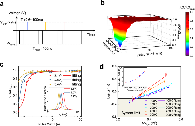
a Schematic of the switching kinetics measurement procedure. Before each measurement, a voltage pulse (Vreset) is used to reset the polarization state of WTe2. Subsequently, the width and amplitude of the switching pulses are varied continuously, while the in-plane conductance of Td-WTe2 is measured continuously. b The response of Td-WTe2 to different pulse parameters at a temperature of 100 K. Note that the voltage unit is VC (coercive voltage extracted from the Goff-Vtg-p loops). c Fitting results of three representative ΔG/ΔGmax vs pulse width curves using the NLS model. The inset shows the Lorentzian distribution of fitted waiting times. d The characteristic switching time, τ0, under different voltages at different temperatures, fitted using the Merz law. The inset shows the anomalous increase of activation field with temperature.
To extract the characteristic polarization switching parameters of Td-WTe2, we fitted the voltage pulse switching curves (three representative fittings are shown in Fig. 2c) using the nucleation-limited-switching (NLS) model for ferroelectric polarization reversal29,30 (fitting with the Kolmogorov–Avrami–Ishibashi model was also conducted but the results were unphysical, see SI section 4 for details). The switching behaviors are well-described by the NLS model, and the waiting time distributions for different Vtg-p magnitudes are plotted in the inset of Fig. 2c. From these fittings, we can extract the characteristic switching time (τ0) of the device under different Vtg-p and temperatures. The results for Device 1 are shown in Fig. 2d and those for Devices 2–4 are shown in SI section 6. To one’s great surprise, the characteristic switching time τ0 over a wide range of Vtg-p apparently increases with increasing temperature, as shown in Fig. 2d. This is completely opposite to the behavior of conventional ferroelectrics, where increasing temperature facilitates polarization switching30,31,32,33. The field dependence of τ0 at a given temperature aligns with the Merz law34. By plotting log(τ0) vs 1/V, we extracted the activation fields (Ea) for reverse domain formation at different temperatures. Again, the activation field increases with temperature as shown in the inset of Fig. 2d (Note that although the dashed line in Fig. 2d was fitted using an exponential function, it is intended solely as a qualitative indicator of the trend, rather than a quantitative fitting model).
Modeling and first principles calculations
The activation field, which quantifies the response of ferroelectric polarization to an applied electric field, is primarily influenced by factors such as temperature, polarization magnitude, and domain wall energy31,33,35. The latter is governed by contributions from polarization gradient energy (dipole-dipole interactions), local energy (as described by the Landau–Ginzburg–Devonshire phenomenological theory), and elastic energy. In conventional ferroelectrics, 180° polarization switching involves the displacement of ions without significant deformation of the adjacent crystal lattice, resulting in the dominance of gradient and local energies within the domain wall energy31. Furthermore, in typical switching measurements, the testing temperatures are usually distant from the Curie temperature, ensuring that neither polarization magnitude nor domain wall energy undergoes significant change. Consequently, prior studies on conventional ferroelectrics usually show a reduction in both the characteristic switching time and the activation field as temperature increases30,31,32,33. What causes the drastically different switching kinetics in Td-WTe2 as compared to those of conventional ferroelectrics? Naturally, we look into the unique vdW structure and “sliding” mechanism for polarization switching, and the semimetallic nature of Td-WTe2 for possible answers. Since the polarization of Td-WTe2 arises due to interlayer charge transfer, temperature may affect the polarization by changing the redistribution of electrons near the Fermi surface. Furthermore, atomic thermal vibrations and the formation of ripples in vdW materials due to thermal perturbations36 may make it more difficult for one layer to slide against its neighboring layers under the same electric field. Considering the simplest bilayer system, the free energy change associated with the formation of the reversed nucleus is as following (See SI section 5 for details):
$$\Delta U=-2{PEab}+a{u}_{2a}+2b{u}_{2b}+a{u}_{2c}$$
(1)
and the expression for the activation field is
$${E}_{a}=\frac{\left({u}_{2a}+{u}_{2c}\right){u}_{2b}}{{k}_{B}{TP}}$$
(2)
where \({u}_{2a}\), \({u}_{2b}\), and \({u}_{2c}\) are linear energy densities of the domain walls for the stretched, twisted, and bent domain walls, respectively (Fig. 3a). The bent and stretched domain walls are perpendicular to the sliding direction, while the twisted domain walls are parallel to the sliding direction. kB is the Boltzmann constant, T is the temperature, and P is the polarization magnitude. This expression is similar to that for conventional ferroelectrics35,37,38.
Fig. 3: Formation of reversed domains and the temperature-dependent polarization switching in Td-WTe2.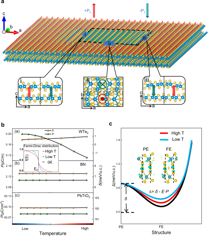
a Schematic illustration of a reversed domain in Td-WTe2, highlighting three types of domain walls: stretched (i), twisted (ii), and bent (iii). The arrows represent local polarization directions. In the stretched domain wall, atomic distances of the upper layer increase. In the bent domain wall, the upper layer bends due to the opposite sliding of neighboring regions. b Influence of temperature on the polarization and energy barriers between opposite polarization states in Td-WTe2, BN, and PbTiO3. For WTe2, increasing temperature reduces polarization and slightly elevates the intrinsic barrier, whereas BN and PbTiO3 retain stable polarization and intrinsic barriers. Here, δ denotes the barrier without an external field. The inset shows how temperature affects the electron distribution near the Fermi level, controlled by the smearing parameter σ. c Under an external electric field E, the switching barrier is defined as ∆ = δ−E · P. The blue line represents low temperature, the red line high temperature, and the black line the intrinsic barrier. The charge density difference demonstrates charge transfer between layers during the ferroelectric phase transition.
We then employed density functional theory (DFT) calculations to investigate how polarization magnitude and energy barriers in bilayer Td-WTe2 depend on temperature. Although DFT treats systems at zero temperature with a step-function Fermi-Dirac distribution, we introduced a smearing technique to approximate finite-temperature effects, where larger smearing values correspond to higher effective temperatures39,40,41. As shown in Fig. 3b, with increasing temperature (smearing values from 0.01 to 0.11), the polarization magnitude of Td-WTe2 decreases monotonically, while the energy barrier between the ferroelectric and paraelectric phases increases slightly. In contrast, typical insulating sliding ferroelectrics, such as bilayer BN, and the conventional ferroelectric PbTiO3, show no notable changes in polarization or barrier upon the same increase in temperature. This distinct behavior likely originates from the semi-metallic nature of Td-WTe2, where the polarization arises from interlayer charge transfer, as shown in the inset of Fig. 3b. As temperature increases, the electron distribution near the Fermi level shifts, reducing the charge transferred between layers and thus lowering the polarization. To illustrate this point clearly, we conducted a detailed analysis of the electronic band structure of WTe2 (Fig. S18) and the projected density of states (PDOS, Table S4). The analysis confirmed the reduction in interlayer charge transfer, supporting the observed decrease in polarization. For a more comprehensive discussion, readers are referred to Section 7 in the Supplementary Information. This reduced polarization affects the switching barrier under an applied electric field. Defining the switching barrier as ∆ = δ − E · P (where δ is the intrinsic energy difference between ferroelectric and paraelectric phases, E represents the electric field, and P denotes the polarization magnitude). We find that while δ increases slightly with temperature, the decrease in P is more significant. Consequently, at a fixed electric field E, higher temperatures lead to larger ∆, making polarization reversal increasingly difficult, as illustrated in Fig. 3c.
Furthermore, for sliding ferroelectrics, the polarization reversal process occurs through the inter-layer sliding displacement between neighboring layers. As the temperature increases, atomic vibrations become more pronounced, leading to an increase in the resistance to inter-layer sliding42. Additionally, thin layers of 2D materials exhibit extremely low out-of-plane bending stiffness, rendering them highly sensitive to thermal perturbations that can induce rippling. As the temperature rises, both the probability and amplitude of ripple formation increase, causing the material to become increasingly wrinkled36. This phenomenon further contributes to the rise in friction as the atomic layers slide against each other43. Thus, the combination of reduced polarization and increased resistance to inter-layer sliding leads to the observed increase in the activation field.
Fatigue resistance of polarization switching in WTe2
Besides switching speed, switching endurance, i.e., fatigue performance of a ferroelectric material is also crucial for potential applications. Earlier studies on twisted bilayer BN and MoS2 suggest that vdW sliding ferroelectrics are highly fatigue resistant23,24. We have conducted fatigue testing on Td-WTe2. Square pulses of ±13 V were applied to the top gate of Device 1 (bottom gate kept at 0 V) at a frequency of 2 × 10⁴ Hz. During the cycling, the in-plane conductance Gon of the device was measured at different stages. As shown in Fig. 4a, there is no changes in the dynamic and static Gon and Goff vs V loops even after 1010 switching cycles. Throughout the entire fatigue testing, there was no significant change in the coercive voltage or the conductance of Td-WTe2 (Fig. 4b). The fatigue-free switching characteristics of Td-WTe2 may be attributed to the difficulty of defect movement during the sliding process and the negligible pinning effect of defects on domain wall motion24.
Fig. 4: Fatigue performance of Td-WTe2.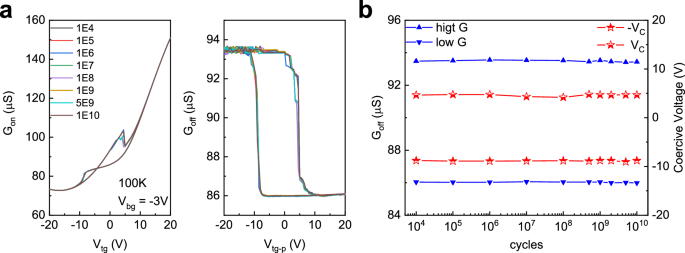
a Response of Gon and Goff to the external electric field at different stages of the fatigue test. Curves of different colors correspond to different numbers of cycles. Measurements were performed at 100 K. b Variation of the coercive voltage and conductance with the number of switching cycles for different polarization directions.