
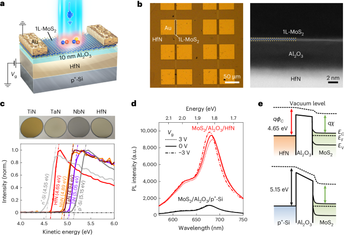
Monolayer MoS2 was synthesized over large areas on c-plane sapphire substrates via CVD (Methods and Supplementary Fig. 1)28 and subsequently transferred onto the target substrates using an Au-assisted dry transfer process. PL spectra collected from 20 randomly selected positions show highly uniform optical properties. The variation in intensity was within 1% across a 1 × 1 mm2 area (Supplementary Fig. 2), and the defect density remained as low as that of mechanically exfoliated samples (~1012 cm−2; Supplementary Fig. 3). The transferred MoS2 was integrated onto a 10-nm-thick Al2O3 dielectric on a conductive HfN gate electrode to form a vertical heterostructure for gated devices. Despite minor lattice distortions associated with the transfer process, the monolayer character of MoS2 was preserved, and the fabricated MoS2/Al2O3/HfN heterostructure was confirmed by high-resolution transmission electron microscopy, as shown in Fig. 1b. The heterostructure interface remained clean and well defined. The integration of large-area, high-quality monolayer MoS2 enables the batch fabrication of field-effect transistor arrays using conventional photolithographic techniques, with uniform channel morphology over millimetre-scale areas.
To investigate the influence of the gate electrode material on the optoelectronic response of the MoS2 heterostructure, we deposited various TMNs (TiN, TaN, NbN and HfN) on p+-silicon with a thickness of 100 nm via sputtering at 800 °C. All TMN films exhibited optically metallic behaviour (Re(ε) < 0) and ultrasmooth surfaces with a root-mean-square roughness of less than 1 nm, with good plasmonic properties across the visible and infrared regimes (Supplementary Fig. 4). We performed ultraviolet photoelectron spectroscopy to quantify the work functions of these TMN films (Fig. 1c). The measured values, in descending order, are 5.05 eV for TiN, 4.94 eV for TaN, 4.89 eV for NbN and 4.65 eV for HfN, which are not very different from previously reported values. Of these, HfN provided the most favourable alignment of the work function (~4.65 eV) with that of CVD-grown monolayer MoS2 (4.48 eV)44, which reduced the interfacial band offset and minimized the undesirable band bending.
To evaluate the effect of gate material on the electrostatic doping, we measured the gate-dependent PL modulation of MoS2 from 0 V to −5 V. As shown in Fig. 1d, the HfN gate produced nearly an order-of-magnitude larger PL enhancement than a conventional p+-Si gate, indicating more efficient electrostatic control, consistent with the different interfacial band alignments (Fig. 1e). The higher work function of p+-Si (~5.15 eV) induced stronger surface band bending in MoS2, which limited the photo-induced carrier accumulation, whereas the lower work function of HfN (~4.65 eV) provided more favourable band alignment for stronger gate-induced charge modulation. Note that the Al2O3 dielectric layers in both the HfN and p+-Si devices were deposited using the same atomic layer deposition process under identical conditions with comparable surface quality and uniformity (Supplementary Fig. 5). Therefore, the observed difference in PL modulation depth arose from interfacial band alignment differences due to the work-function contrast between HfN and p+-Si, rather than variations in the dielectric layer.
To explore the mechanism underlying the gate-dependent PL modulation in monolayer MoS2 for various gate materials, we investigated the evolution of the PL spectra under various gate biases. Figure 2a presents PL colour maps of monolayer MoS2 on the Al2O3/HfN and Al2O3/p+-Si platforms as a function of the gate voltage (Vg), which was swept from −5 V to +5 V. The HfN-gated device showed a pronounced PL intensity change and emission redshift, evidencing effective gate-controlled excitonic modulation, whereas the p+-Si platform exhibited little response under the same bias conditions. The gate-tuned PL spectra were deconvolved into several Lorentzian components (Supplementary Fig. 6), corresponding to neutral excitons (X), negatively charged trions (X−) and defect-induced localized states. The progressive redshifting of the PL peak in the HfN-gated device can be attributed to increasing photo-excited charge accumulation in the monolayer MoS2 channel with a positive gate bias. This interpretation is supported by capacitance–voltage (C–V) measurements (Fig. 2b and Supplementary Fig. 7), from which the induced carrier concentration (N) was estimated using the expression
$$\,{N}_{\mathrm{induced}}({V}_{{\rm{g}}})=\frac{1}{q}{\int }_{{V}_{\min }}^{{V}_{{\rm{g}}}}C({V}_{{\rm{g}}}^{{\prime} })\,{\rm{d}}{V}_{{\rm{g}}}^{{\prime} },$$
(1)
where q, C and Vg represent the elementary charge, measured capacitance and applied gate voltage, respectively. Note that the high-voltage terminal was connected to the gate here, whereas the low-voltage terminal was connected to the source and drain. At Vg = +5 V, the HfN gate induced a photo-excited charge concentration of ~2.3 × 1012 cm−2, which is in close agreement with the theoretical calculations (Supplementary Information Section 4). In comparison, the p+-Si gate induced a photo-excited charge concentration of only ~1.2 × 1012 cm−2 under the same bias, confirming the superior electrostatic control provided by the HfN platform. Gate-dependent reflectance contrast spectra at 85 K and 300 K confirmed the effective electrostatic control of excitonic states in the MoS2/Al2O3/HfN heterostructure, which had sharper and higher-contrast features at 85 K due to the reduced thermal broadening (Supplementary Figs. 8 and 9).
The enhanced gate-tunable photo-excited charge modulation is corroborated by the band diagrams shown in Fig. 2c. Under equilibrium conditions, HfN has a slightly higher work function than MoS2, leading to modest upward band bending and photo-induced hole accumulation at the interface. Although these holes can bind with neutral excitons to form positively charged trions (X+), the intrinsic n-type nature of MoS2, which is characterized by an excess of free electrons, makes the formation of positive trions less favourable45. Moreover, the relatively low binding energy of positive trions may lead to their rapid dissociation, causing their signal in the PL spectrum to be obscured46. Upon application of a positive gate voltage, the electrostatic potential of HfN is lowered, thereby reversing the band-bending direction and promoting notable photo-induced electron accumulation. This process facilitates the formation of stable negatively charged trions (X−), which is consistent with the observed PL evolution shown in Fig. 2a.
Fig. 2: Working mechanism of gate-controlled PL in monolayer MoS2 on a HfN gate.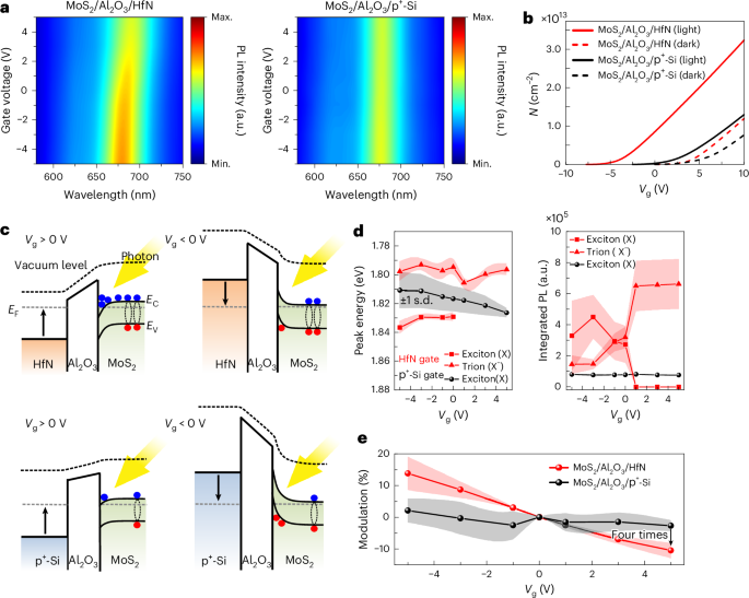 The alternative text for this image may have been generated using AI.
a, Colour maps of PL spectra of monolayer MoS2 on Al2O3/HfN and Al2O3/p+-Si under various gate biases. The HfN platform showed strong gate-dependent PL intensity and peak shifts, indicating effective excitonic modulation, whereas no gate-dependent emission was observed from the p+-Si platform. b, Calculated carrier density in monolayer MoS2 on HfN and conventional p+-Si gates under light and dark conditions. The enhanced photocurrent under illumination confirms the photoresponse, and the threshold shift highlights the gate-induced modulation of charge carriers. c, Band diagrams of MoS2 on HfN and p+-Si gates under positive and negative gate voltages. The lower work function of HfN enabled stronger electrostatic electron accumulation at positive gate bias compared with p+-Si, leading to more efficient band bending and inducing more photocarriers into MoS2. d, Extracted PL peak energy and peak intensity as functions of gate voltage. HfN-gated devices showed pronounced gate-dependent exciton and trion modulation, in contrast to the minimal changes observed in the p+-Si control. Data points represent the mean values from three independent devices, and the shaded regions indicate ±1 standard deviations. e, PL modulation ratio of monolayer MoS2 emission on different gate platforms under various gate voltages. Max., maximum; Min., minimum.
By contrast, p+-Si had a high work function, and the MoS2 channel experienced stronger upward band bending at equilibrium and less effective photo-induced charge accumulation under a positive gate bias. This resulted in weaker trion formation and minimal PL modulation. We quantified the effects in Fig. 2d,e by plotting the extracted PL peak positions and integrated intensities of exciton (X) emission and negatively charged trion (X−) emission as a function of the gate voltage. Shaded regions denote the standard deviation obtained from measurements across three independent device locations on the scalable MoS2 films, and these reflect uniform device performance.
To verify batch-to-batch reproducibility, we performed gate-tunable emission measurements on other scalable monolayer MoS2 samples and found that, despite slight variations in the initial carrier concentration, the overall trends remained consistent. Averaged results from ten independently measured devices, with error bars denoting the standard deviation, confirm the statistical reproducibility of the spectral shifts and gate-dependent trion modulation (Supplementary Figs. 10–13).
The energy splitting between the X and X− peaks yielded a trion binding energy of 34 meV, which is consistent with previously reported values (26–32 meV)47. The slight shift in the neutral exciton peak on the HfN platform compared with that on the p+-Si platform is attributed to the substrate45. Under positive gating, the PL emission of MoS2 on HfN was dominated by trion X− recombination, whereas minimal variation was observed for the p+-Si control.
To evaluate the optical modulation efficiency, we define the PL modulation ratio as
$$\mathrm{Modulation}\,\mathrm{ratio}=\frac{P\left({V}_{{\rm{g}}}\right)-P\left({V}_{{\rm{g}}}=0\right)}{P\left({V}_{{\rm{g}}}=0\right)},$$
(2)
where P represents the PL peak intensity. As shown in Fig. 2e, the HfN-gated device had a PL peak modulation ratio of 10.4% at Vg = +5 V, which is more than four times greater than that for the gated p+-Si counterpart (2.6%).
To further tailor the light–matter interactions in monolayer MoS2, we developed four HfN-gated device architectures incorporating surface passivation and NPoM plasmonic nanocavities (Fig. 3). An unpassivated monolayer MoS2/Al2O3/HfN device (Fig. 3a) showed strong gate-dependent PL modulation but suffered from surface-related losses. Adding a 10-nm Al2O3 passivation layer suppressed surface traps, yet reduced charge transfer and PL modulation (Fig. 3b). Interestingly, the PL response under a gate bias became inverted relative to that of an unpassivated device. This inversion is attributed to electron trapping in the Al2O3 capping layer under a positive bias, which suppressed the formation of negatively charged trions (X−), leading to diminished PL at high gate voltages. To harness the plasmonic-induced PL enhancement, we fabricated gold nanodisc (AuND) arrays (Methods) on top of the MoS2/Al2O3/HfN heterostructure to form NPoM nanocavities. In the absence of a passivation layer (Fig. 3c), direct integration of the Au nanostructures with MoS2 resulted in severe PL quenching across all bias conditions. This quenching arose from non-radiative energy transfer48, which dominated any enhancement provided by the plasmonic near fields. Nevertheless, some gate tunability was retained because of the preserved electrostatic access from the HfN back gate. Strikingly, the combined implementation of both Al2O3 surface passivation and NPoM plasmonic nanocavity fabrication (Fig. 3d) yielded a synergistic enhancement in the PL output and gate responsiveness. The passivation layer suppressed metal-induced quenching, and the plasmonic AuND array enhanced local fields and increased the radiative recombination rate, together yielding the strongest PL intensity and gate-tunable modulation among all tested configurations. These results reveal that proper surface engineering, including charge trap suppression and resonant nanophotonic design, is essential for maximizing both the intensity and gate tunability of emission.
Fig. 3: Engineering surface passivation and plasmonic resonance to modulate and enhance the light–matter interaction in monolayer MoS2.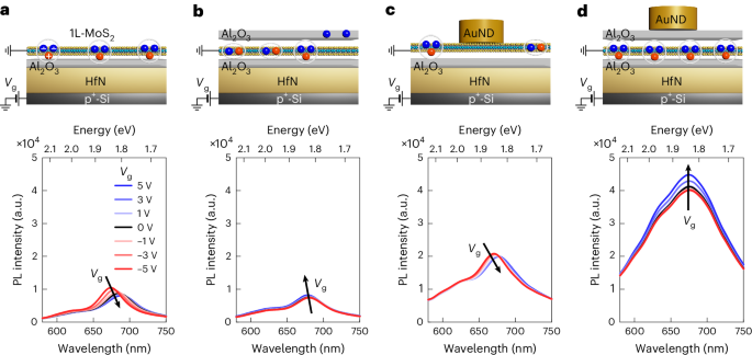 The alternative text for this image may have been generated using AI.
a–d, Top: schematic illustrations of different device architectures integrating monolayer MoS2 on Al2O3/HfN-gated heterostructures. Bottom: corresponding PL spectra for each configuration under identical excitation conditions a, Gate-tunable PL spectra of monolayer MoS2 with an HfN bottom gate. b, Gate-dependent PL spectra of monolayer MoS2 on Al2O3/HfN with an Al2O3 passivation layer leading to exciton quenching. c, Gate-dependent PL spectra of monolayer MoS2 on Al2O3/HfN with Au plasmonic nanostructures. d, Gate-tunable PL spectra of monolayer MoS2 on Al2O3/HfN with an Al2O3 passivation layer and Au plasmonic nanostructures, resulting in giant gate-tunable emission. The passivation layer minimizes charge traps and environmental doping, and the plasmonic nanostructure enhances the light–matter interaction. Devices with plasmonic nanostructures and proper passivation exhibited significantly enhanced PL intensity, spectral purity and tunability, which highlights the synergistic effects of local field enhancement and exciton stabilization via surface passivation.
To investigate the role of the NPoM plasmonic nanocavities in enhancing the gate-tunable excitonic emission in monolayer MoS2, we designed and fabricated AuND arrays with various diameters on Al2O3-passivated MoS2/Al2O3/HfN heterostructures. Figure 4a is a spatially resolved PL colour map of monolayer MoS2 in the Al2O3-passivated MoS2/Al2O3/HfN heterostructure. A portion of the surface is covered by AuND arrays. The region with AuND coverage exhibits a markedly enhanced PL intensity, which is attributable to strong light confinement in the nanogaps between the AuNDs and the HfN backplane. These gaps form NPoM plasmonic cavities. Optical microscopy and scanning electron microscopy images confirm the uniformity and geometry of the plasmonic arrays.
We subsequently examined the spectral response of these structures under various gate biases. As shown in Fig. 4b, the gate-dependent PL spectra of the NPoM-coupled monolayer MoS2 display simultaneous modulation of both the neutral exciton (X) and trion (X−) features. Compared with the unpatterned region, the plasmonic nanostructures induce both spectral redshifts and intensity enhancements. These enhancements were most pronounced when the plasmon resonance, tuned via the nanodisc diameter, spectrally overlapped the excitonic states of MoS2. This spectral matching enabled efficient exciton (trion)–plasmon coupling and enhanced the radiative recombination via the Purcell effect49,50. The calculated reflection spectra (Fig. 4b) reveal that increasing the AuND diameter resulted in a systematic redshift of the localized surface plasmon resonance, allowing precise spectral alignment with the MoS2 excitonic states.
To gain insights into the near-field enhancement mechanism, we performed finite-difference time-domain simulations of the electric field distribution in resonant (D = 70 nm) and non-resonant (D = 40 nm) NPoM plasmonic nanocavities at 660 nm (Fig. 4c). The calculated |E|2/|E0|2 profiles show pronounced field confinement within the Al2O3 spacer and at the MoS2 interface in the resonant cavity, in contrast to the weaker and more delocalized fields observed in the non-resonant structure. Thus, the enhanced local field increased absorption in the MoS2 layer (Supplementary Fig. 14).
Fig. 4: Resonant plasmonic nanostructures enhance gate-tunable emission in monolayer MoS2.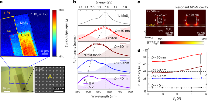 The alternative text for this image may have been generated using AI.
a, Top: PL mapping of monolayer MoS2 partially covered by an AuND array. Enhanced emission was observed in the AuND region due to the light–matter interaction induced by the NPoM plasmonic nanocavity. Bottom left: optical microscopy image indicating the mapping region. Bottom right: scanning electron microscopy image of the AuND array, which had a diameter of 70 nm and periodicity of 200 nm. b, Gate-dependent PL spectra (solid and dashed curves) from the MoS2 on Al2O3/HfN and the MoS2 coupled with an NPoM nanocavity. Simulated reflection spectra (shaded profiles) from an AuND array with various geometries. The vertical dashed line marks the MoS2 A-exciton emission. There is a gradual increase in the redshift of the PL spectra and reflection dip (dashed guide) with increasing diameters of the AuND array. Spectral tuning and intensity amplification indicate efficient exciton–plasmon coupling and carrier-controlled trion formation. c, Calculated electric field distributions of NPoM nanocavities with a resonant plasmonic nanostructure (right) and a non-resonant plasmonic nanostructure (left) at 660 nm. The panel illustrates the stronger field confinement and enhancement for the resonant plasmonic nanostructure, which more effectively couples with the exciton and trion. d, Gate-dependent PL spectra of monolayer MoS2 coupled with NPoM nanocavities formed by AuNDs with different diameters, demonstrating the enhanced modulation depth enabled by the resonant coupling between the NPoM mode and the excitonic level. The non-resonant plasmonic nanostructure shows minimal tunability, confirming the critical role of plasmon–trion coupling in enhancing light–matter interactions.
The impact of this field enhancement on the electrical tunability is summarized in Fig. 4d. Devices incorporating 70-nm AuNDs exhibited a greatly increased PL modulation depth as a function of the gate voltage, with both the X and X− features showing gate-dependent peak shifts and PL intensity changes. By contrast, devices with non-resonant nanodiscs (40 nm) showed negligible PL modulation, which confirms the critical role of the exciton (trion)–plasmon coupling and spectral overlap in enabling efficient gate control. These observations confirm that only resonant NPoM configurations yield simultaneous optical enhancement and giant gate-tunable PL, and they demonstrate a synergistic interplay between plasmonic confinement and gate-induced carrier dynamics. Numerical simulations indicate a localized Purcell enhancement of up to 175 in the NPoM nanocavity (Supplementary Fig. 15), which reinforced the excitonic emission. The device maintained stable PL output with <3% degradation over 1 week and with robust room-temperature performance despite thermally induced PL quenching with increasing temperature to 700 K due to intrinsic MoS2 degradation (Supplementary Figs. 16 and 17). As high-temperature quenching is inherent to 2D excitonic materials, our focus here is on demonstrating robust room-temperature tunability and plasmonic enhancement over wafer-scale areas for practical photonic and optoelectronic applications.
Figure 5 compares the figure of merit (FOM) and tunable region of various gate-tunable devices based on monolayer TMDCs. The FOM is defined as
$$\mathrm{FOM}=\frac{{P}_{\max }}{{P}_{\min }}\times \frac{1}{{V}_{{\rm{g}}}},$$
(3)
where a higher FOM indicates stronger PL modulation achieved with a lower gate voltage (Supplementary Table 1). For monolayer MoS2 devices, although exfoliated flakes offer strong modulation (Fig. 5), their tunable area is small and not scalable. In this work, we employed CVD-grown large-area single-crystal MoS2, whose defect density can be comparable with that of exfoliated flakes, thus ensuring high optical quality. This wafer-scale MoS2 enables gate-tunable modulation over much larger regions and allows the simultaneous operation of several devices. The designed HfN-gated device exhibited a FOM of ~0.11. We believe this value can be increased by mitigating structural defects. Notably, the current device had a tunable emission area of ~5,000 μm2, which is at least one order-of-magnitude larger than that reported for most exfoliated or CVD-grown monolayer TMDC devices. Hence, our results highlight a robust design strategy for enhancing and modulating the light emission in monolayer TMDCs through the careful spectral engineering of plasmonic nanostructures.
Fig. 5: Benchmarks of tunable regions for monolayer TMDC devices.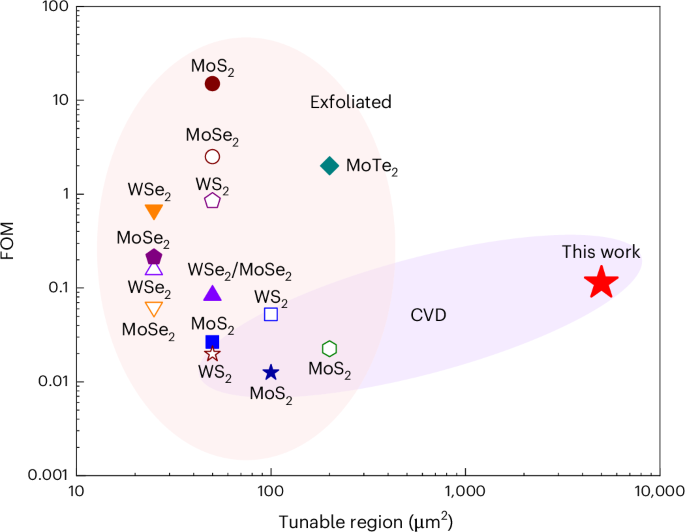 The alternative text for this image may have been generated using AI.
Benchmarking the electrostatic tunability of various monolayer TMDC systems based on the FOM and tunable region. The pink-shaded region corresponds to exfoliated monolayers, which generally exhibit high FOM but limited tunable area. The other shaded region represents CVD-grown monolayers, which have larger scalable areas but typically lower FOM. The star highlights the result of this work, which employs HfN as the gate electrode with an NPoM cavity to achieve both high tunability and a large tunable region.
The measured external quantum efficiency of our trion-dominated emission is intrinsically low (~0.8%; Supplementary Fig. 18), consistent with the reported PL quantum yield below 8% for exfoliated monolayer MoS2 (ref. 10). Such tunability originates from trions, whose strong sensitivity to carrier-density modulation underlies the pronounced gate-dependent optical behaviour of monolayer MoS2. Many-body perturbation calculations further reveal that the gate modulates the trion binding energy. The predicted modulation aligns well with the experimentally observed gate-dependent PL redshift and intensity variation (Supplementary Fig. 19). Combined with macroscopic quantum electrodynamics, the theoretical PL rates can be separated into the density of states of excitons and trions and the Purcell effect. Taken together, the theoretical and experimental findings provide a coherent and self-consistent picture of the plasmon–trion coupling mechanism. The combination of trion–plasmon coupling and electrical doping control enables highly tunable, scalable and efficient 2D light sources for on-chip optoelectronic integration.