
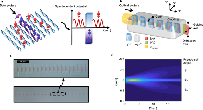
Pseudo-spin guiding mechanism
We can describe the process of paraxial SFG process in the undepleted pump approximation using the coupled wave equations, written as an optical pseudo-spin transport equation, while assuming a phase-matched interaction20,21,22,23 (see Supplementary Note 1 for derivation):
$${{\rm{i}}}\frac{{{\rm{d}}}}{{{\rm{dz}}}}{{\boldsymbol{\Psi }}}=\left(\frac{{{{\bf{p}}}}_{{{\rm{T}}}}^{2}}{2{{\rm{k}}}}-{{\boldsymbol{\sigma }}}\cdot {{{\bf{M}}}}_{{{\bf{T}}}}\right){{\boldsymbol{\Psi }}}$$
(1)
where \({{\boldsymbol{\Psi }}}={\left(\sqrt{\frac{{n}_{i}}{{\omega }_{i}}}{A}_{i},\sqrt{\frac{{n}_{s}}{{\omega }_{s}}}{A}_{s}\right)}^{T}/\sqrt{N}\), with \(N={n}_{i}{\left|{A}_{i}\right|}^{2}/{\omega }_{i}+{n}_{s}{\left|{A}_{s}\right|}^{2}/{\omega }_{s}\) such that \({{{\boldsymbol{\Psi }}}}^{{{\boldsymbol{{\dagger} }}}}{{\boldsymbol{\Psi }}}=1\), is the (rotating frame) spinor comprising the idler and signal envelopes, where \({A}_{i}\) and \({A}_{s}\) are the complex amplitudes of the idler and signal, respectively. \(k \sim {k}_{i},{k}_{s}\) is a mean wavenumber (due to the long pump wavelength approximation), \({{\boldsymbol{\sigma }}}=\left({\sigma }_{x},{\sigma }_{y},{\sigma }_{z}\right)\) is the Pauli matrix vector, \({{{\bf{p}}}}_{T}=-i{{{\boldsymbol{\nabla }}}}_{T}\) is the transverse momentum operator in position-space representation, and the analogous transverse magnetization vector \({{{\bf{M}}}}_{{{\bf{T}}}}\) is determined from the nonlinear interaction parameters:
$${{{\bf{M}}}}_{{{\bf{T}}}}=\hat{{{\rm{x}}}}\kappa \cos \left(\phi \right)+\hat{{{\rm{y}}}}{{\rm{\kappa }}}\sin \left(\phi \right)$$
(2)
where \(\kappa \propto |{\chi }^{\left(2\right)}{A}_{p}|\) is the nonlinear coupling (see full expression in Supplementary Note 1), \({\chi }^{\left(2\right)}\) is the second-order susceptibility, and \({A}_{p}\) is the pump amplitude. Under our analogy, the pure idler (\({\omega }_{i}\)) or signal (\({\omega }_{s}\)) frequencies correspond to the PS eigenstates along the \(z\)-direction (optical axis), which we denote \(\bar{|}\psi i\rangle={A}_{i}\otimes |{\omega }_{i}\rangle\) and \(\left|{\psi }_{s}\right\rangle={A}_{s}\otimes \left|{\omega }_{s}\right\rangle\), respectively, including both the frequency and the spatial envelope of the signal and idler. \(\phi\) is the phase difference between the pump phase and the periodically-poled nonlinear crystal initial phase. Here, the PS eigenstates that point along the transverse magnetization vector comprise an equal superposition of \(\left|{\psi }_{i}\right\rangle\) and \(\left|{\psi }_{s}\right\rangle\) with either 0 or \(\pi\) relative phase (assuming \(\phi=0\)):
$$\left|{\psi }_{\pm }\right\rangle=\frac{\left|{\psi }_{i}\right\rangle \pm \left|{\psi }_{s}\right\rangle }{\sqrt{2}}$$
(3)
Equation (1) is then diagonalized using a transformation matrix, where \(|{\psi }_{\pm }\rangle\) now acting as PS up and down. Next, we consider the following spatially varying duty cycle (Fig.1b):
$${d}_{x}=\left\{\begin{array}{cc}0.5,& \left|x\right| < a\\ 0,& {else}\end{array}\right.$$
(4)
where \(2a\) is the width of the designated PS waveguide (acting as an analog photonic core). Namely, a narrow strip of a modulated second-order nonlinearity that allows an efficient process through quasi-phase matching (QPM)24. Assuming an efficient first-order (QPM) interaction, the former duty cycle results in the following transverse magnetization pattern:
$${{{\bf{M}}}}_{{{\bf{0}}}}\left(x\right)=\left\{\begin{array}{cc}+{M}_{0}\hat{{{\bf{x}}}},\, & \left|x\right| < a\\ 0,& {else}\end{array}.\right.$$
(5)
Equation (1) can now be rewritten as two decoupled equations for the PS up and down eigenstates:
$$i\frac{d}{{dz}}\left|{\psi }_{\pm }\right\rangle=\left(\frac{{{{\bf{p}}}}_{T}^{2}}{2k}\mp {{{\bf{M}}}}_{{{\bf{0}}}}\left(x\right)\right)\left|{\psi }_{\pm }\right\rangle$$
(6)
Which is analogous to the Schrodinger Equation of a particle in a spin-dependent potential, governed by \({\kappa=M}_{0}{\propto |\chi }^{\left(2\right)}{A}_{p}|\). To find the eigenvalues of the presented structure, we solve the ‘z’ independent equation and obtain the transcendental equation whose graphical solution appears in the Supplementary Note 1. As can be seen in Fig. 1d, the input idler beam, composed of a superposition of \({|\psi }_{+}\rangle\) and \(\left|{\psi }_{-}\right\rangle\) eigenstates, propagates in two ways. First, the \(|{\psi }_{+}\rangle\) component is fully guided inside the effective PS waveguide, in the ‘X’ axis, since it evolves in a finite well potential. Second, the \(|\psi \_\rangle\) component is scattered and diffracted, adjacent to the PS waveguide structure, since it is scattered from a potential barrier.
The relative ease of the guiding mechanism (i.e., only a narrow strip of periodic modulation) enables us to envision and design components similar to conventional photonic circuits1, but for frequency superposition light beams. Here, we designed a directional coupler, made from two adjacent PS waveguides. This constitutes two spin-dependent potential wells where the PS can tunnel through the barrier, similar to other systems that can be modeled as a double potential well25.
We note that while our theoretical model captures the confinement, coupling and scattering of the PS waveguide, its accuracy depends on the long pump wavelength approximation made in deriving Eq. 6. Therefore, in the presented experiment, while guiding and tunneling are observed both in simulation and experiment, it does not follow precisely the analytic model of Eq. 1. This means that when the approximation is crude, as in our experimental case, detailed simulations are more accurate for prediction of the light behavior. This difference is further discussed in the Supplementary Note 2.
Single pseudo-spin waveguide
We fabricated a narrow (in the ‘X’ direction, see Fig. 1c) custom PPKTP crystal whose width (‘X’ axis, the guiding axis) and length (‘Z’ axis, the propagation axis) are 14 µm and 25 mm, respectively. The average poling period of the crystal was designed to be 15.2 µm, which phase-matched the SFG process at a temperature of 58°, a temperature bandwidth of 2°, and a wavelength bandwidth of ~1.2 nm in the idler frequency (see supplementary Note 10). A 1550 nm CW idler was focused to a ~30 µm waist at the input facet of the crystal, and a 1064.5 nm 1.3 ns, pulsed pump beam was concentrated to a 450 µm waist, hence serving as a wide pump beam (Fig. 2a). The output facet of the crystal was imaged using a single lens, while filtering the pump and idler wavelengths. We note that the idler part of the eigenstate is hidden inside the filtered idler wavelength CW. The results for the single PS waveguide are shown in Fig. 2. Clearly, the generated eigenstate beam is guided along the ‘X’ axis, and freely diffracts along the ‘Y’ axis. Next to the guided eigenstate is the spatially scattered eigenstate signal beam, which is not guided. This is depicted in Fig. 2b, c for the experiment and simulation, respectively. The radius of the guided eigenstate signal along the ‘X’ axis is ~24 µm, nearly five times narrower than the signal output width of a regular, 25 mm, PPKTP crystal, which is measured to be around 113 µm, as shown in Fig. 2d. The observed guiding in the ‘X’ axis is the confinement of the PS \(|{\psi }_{+}\rangle\) beam inside the spin-dependent potential, and the scattered beam is the scattered PS \(|{\psi }_{-}\rangle\), much like charged electrons scatter from a Coulomb potential barrier. Interestingly, for an input pump power of 34 MW/cm2, the insertion loss is estimated to be ~1 db, which is comparable to regular nonlinear waveguides, and is attributed to low roughness backscattering. In addition, the mode overlap in the ‘X’ axis is ~97.5% (see Supplementery Note 10 for more metrics).
Fig. 2: Experimental results of the guiding and scattering of |ψ± >.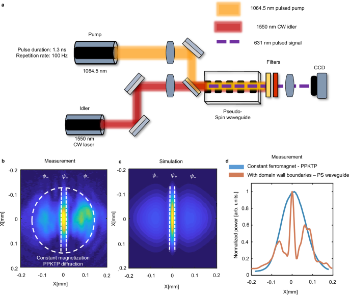
a An Nd:YAG 1064.5 nm pulsed laser (pump) is focused to a waist of ~450 µm inside the PS waveguide, hence can be assumed as a plane wave, with a peak power of 14 MW/cm2. Increasing the pump power resulted in a slightly increased separation (Supplementary Materials). Through a dichroic mirror (DM), the 1550 nm continuous wave (CW) laser is focused to ~30 μm at the PS waveguide input facet. The PS waveguide is mounted on an oven with a temperature controller (58°). The pump and signal beams are filtered, and the output facet is imaged using a lens. The signal is recorded using a CCD camera. Experimental b and simulated c near field images of the signal field at the output facet, showing the guided eigenstate \(\left|{\psi }_{+}\right\rangle\) in the middle, fully guided along the ‘x’ axis and freely propagating along the ‘y’ axis, as well as the scattered, unguided eigenstate \(\left|{\psi }_{-}\right\rangle\). The dashed white circle represents the calculated beam size in the case of a homogeneous PPKTP crystal, without guiding. The dashed white lines mark the region along ‘X’ of the PS waveguide. d Summation (along the ‘Y’ axis) of the output near field. Comparison between the PS waveguide (orange) and a 1D PPKTP signal output (blue). The waist of the guided mode is ~5 times narrower than the homogeneous PPKTP signal output waist.
Next, we show that it is possible to excite mainly the guided eigenstate, therefore verifying the two-color nature of the waveguide, by inserting a frequency superposition state as input to the PS waveguide. To do so, we used an adiabatic frequency converter (AFC)20,26 to coherently generate an approximate superposition of the two in-phase idler-signal frequencies \(|{\psi }_{+}\rangle\). The AFC was placed before the focusing spot of the idler beam, such that both the idler and signal are roughly focused at the waveguide input facet (Fig. 3a). The pump peak power is 34 MW/cm2. Figure 3b shows the signal near field, similar to Fig. 2. As can be seen, the amount of guided peak power in Fig. 3b is significantly larger compared to the scattered peak power. The waist along the ‘X’ axis is ~12 µm, compared to the 58 µm along the freely propagating ‘Y’ axis. Therefore \(|{\psi }_{+}\rangle\) is guided through the device and corresponds to ~39% of the generated signal power. Importantly, this is not always the case; Different combinations of \(|{\psi }_{i}\rangle\) and \(|{\psi }_{s}\rangle\) will generate a similar pattern to Fig. 2a, a guided and non-guided mode. To control the relative phase, we used the natural, slightly wedged structure of the AFC polished output facet. The AFC exhibits a phase difference in the poling structure across the ‘X’ direction because the polished edge of the crystal is not parallel to the ferroelectric domain walls27,28. Therefore, the three waves accumulate slightly different phases at the edges of the crystal. This phase difference corresponds to a phase shift between the generated signal and the idler due to the material dispersion. Therefore, when the signal is generated in different locations along the ‘X’ axis across the AFC (Fig. 3a), it will gain a different relative phase with respect to the signal. Specifically, we used two locations where the measured length difference between them is ~4 µm (1 μm at the beginning of the adiabatic crystal and 3 μm at the end) (see methods). To experimentally utilize this asymmetry, we displaced the location of the waveguide crystal transversely and moved the displacement stage of the oven to the new location. Therefore, the light beams enter the PS guiding crystal in the same place, while accumulating different phases. As can be seen in Fig. 3c, when the three waves (pump, idler, and signal) accumulate different phases, a different power distribution is present, where now, the guided power is ~21% (instead of 39% when the input was \(|{\psi }_{+}\rangle\)). The experimental comparison between the two cases can be seen in Fig. 3d. To verify this behavior, the experiment was simulated using two cascaded processes, an adiabatic converter (see Methods), and a PS waveguide, with a pump and idler as input. Figure 3e shows a similar scenario to Fig. 3b, with the simulated guided signal power corresponding to 38% of the overall signal power. We note that this simulation was simulated in the non-ideal scenario due to differences in the Sellmeier equations, non-ideal focusing, and length difference measurement (see Supplementary Note 3). Taking these into account, we find good agreement between simulation and experiment. Figure 3f shows the same simulation but with a path length difference of ~3 µm at the end of the adiabatic converter (due to experimental non-idealities, see Supplementary Note 3). Here, the guided power corresponds to 20% of the overall signal power, which is similar to the experiment. Figure 3g shows a cross-section comparison after summation along the ‘Y’ axis. As expected, the scattered power is substantially higher, verifying the importance of the relative phase between the participating wavelengths.
Fig. 3: All-optical control over PS waveguide.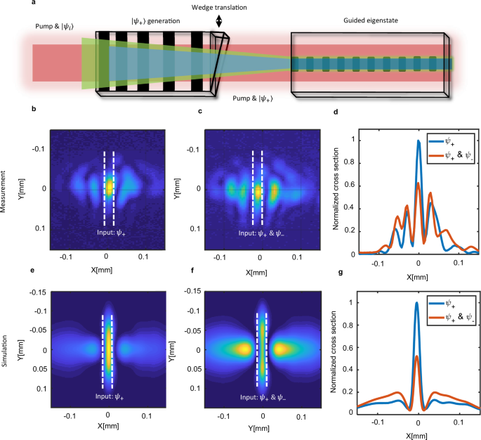
a Schematic illustration of creating a PS waveguide eigenstate. The wide pump (red) and idler (green) beams are focused on the crystal with the PS waveguide structure through the wedged adiabatic converter, generating the |\({\psi }_{+}\)〉 eigenstate. The eigenstate |\({\psi }_{+}\) 〉 is then guided through the PS waveguide structure, resulting in a decreased scattered |\({\psi }_{-}\)〉. b Near field image of the signal field, where most of the power is guided through the structure. c Same as b but with a path difference of 3 μm in the adiabatic converter stage. d Corresponding experimental cross-section. Blue curve corresponds to the results presented in (b), while the orange curve corresponds to the results presented in (c). e–g Simulation results of the experimental results in panels (b–d).
Pseudo-spin directional coupler
The concept of PS guiding is not limited to single waveguides. To demonstrate it, we fabricated a PS directional coupler, made from two adjacent and parallel PS waveguides (Fig. 4a), and then used the same idler input as described before, with a peak power of 34 MW/cm2. When entering from Port 1, \({|\psi }_{+}\rangle\) tunnels to Port 2 (Fig. 4c) and \(\left|{\psi }_{-}\right\rangle\) is scattered. Then, the same crystal was displaced ~30 µm, such that now the input idler beam enters from port 2. As expected, the signal tunneled to port 1 (Fig. 4d). At the edges of Fig. 4c, d, the signal of the scattered \({\psi }_{-}\) can be seen. Figure 4e, f shows the corresponding simulation results of the output signal field. The coupling efficiency of the PS coupler is extracted for Fig. 4 and stands at 62% (see Supplementary Note 10). To gain more insights into the tunneling mechanism, we simulated the propagation inside the structure (Fig. 4b). Similarly to the single waveguide design, the beam experiences scattering and confinement due to the input beam being a superposition of the two eigenstates (\(|{\psi }_{i}\rangle \propto |{\psi }_{+}\rangle+|{\psi }_{-}\rangle\)). Interestingly, as can be seen in Fig. 4b, after the initial scattering and tunneling, the eigenstate (that includes two wavelengths—the signal and the idler) tunnels back again to the first PS waveguide, much like light tunnels in conventional directional couplers (or particles tunnel in two finite potential wells, see Supplementary Note 7).
Fig. 4: PS directional coupler.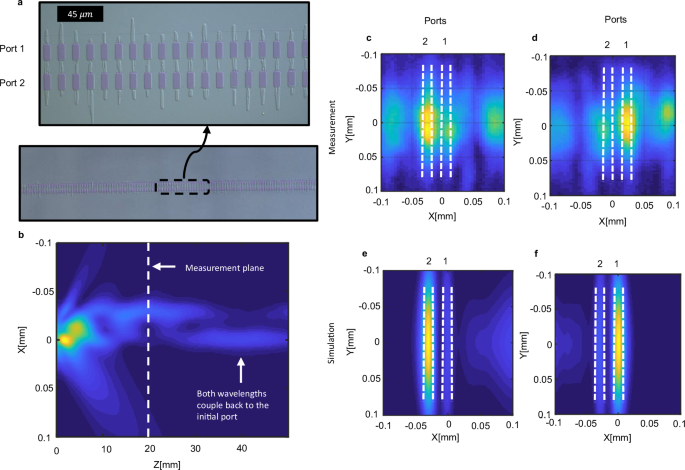
a Microscope top image of the fabricated PS directional coupler after selective etching. The purple color depicts the designed pattern. b Simulated cross-section of the propagation inside the NLPC for an idler input, showing the propagation of both signal and idler. After the scattered eigenstate is scattered from the lower PS waveguide, the guided eigenstate tunnels to the upper waveguide. Then, it tunnels back to the first lower waveguide. The white dashed line marks the experimentally measured crystal length. c Near field image of signal field at the output facet showing the guided eigenstate, |\({\psi }_{+}\)〉 port 2, after tunneling from port 1. Similar to the single waveguide case, the eigenstate is guided along the ‘X’ axis and freely propagates along the ‘Y’ axis. The light at the edges corresponds to the scattered eigenstate |\({\psi }_{-}\) 〉. d Same as panel c, but now the input beams enter from port 2, obtaining tunneling from port 2 to port 1. e, f Simulation results for (c, d). Similarly, to the experiment, due to tunneling of the guided PS between the two ports, a small portion of the signal power can be seen at the input port (either port 1 in panel e or port 2 in panel (f)).