
Hardware-based neural network simulations
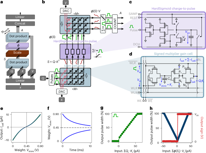
We implement the sliding window attention by masking the elements of S outside the sliding window (blank spaces in the example Fig. 1). The HardSigmoid charge-to-pulse circuit is modeled by the equation
$$\phi (S)=\left\{\begin{array}{ll}{T}_{{\mathrm{max}}}\quad &{\rm{if}}\,S\ge {S}_{{\mathrm{sat}}}\\ \frac{{T}_{{\mathrm{max}}}}{{S}_{{\mathrm{sat}}}}S\quad &{\rm{if}}\,0 < S < {S}_{{\mathrm{sat}}}\\ 0\quad &{\rm{if}}\,S\le 0\end{array}\right.,$$
(3)
where Tmax = 15 ns is the maximum pulse length for the input pulse generators. The input queries Q are quantized in 16 levels between 0 and 1, the stored K and V projections are quantized in 8 levels between 0 and 0.9, and the outputs of the second dot product are quantized in 32 levels between −1 and 1. The quantized models (linear intermediate hardware model and nonlinear hardware model) are trained with quantization aware training48: quantization is done only in the forward pass and the backward pass is done in full precision.
For the nonlinear model of the gain cell, the third-order polynomials
$$\begin{array}{r}S=\mathop{\sum }\limits_{i}^{3}\mathop{\sum }\limits_{j}^{3-i}Q\cdot {\left({K}^{T}-{K}_{{\mathrm{offset}}}\right)}^{i}{V}_{{\mathrm{in}}}^{\,j}{C}_{i,\,j}\\ A=\mathop{\sum }\limits_{i}^{3}\mathop{\sum }\limits_{j}^{3-i}\phi \left(S\right)\cdot {\left(V-{V}_{{\mathrm{offset}}}\right)}^{i}{V}_{{\mathrm{in}}}^{\,j}{C}_{i,\,j}\end{array}$$
(4)
are used with S and A as the outputs, Q and ϕ(S) the input pulse width, K and V the stored voltage, the constant Vin = 0.9 V is the input voltage of the cell applied at the word line read (WLR) ports, the constant yoffset = 0.45 V corresponds to half the supply voltage (VDD/2), and Ci,j as fit parameters from the curve Fig. 1e. To speed-up computation during training, we compute all the tokens in parallel with \(Q\in {{\mathbb{R}}}^{T,D}\), \({K}^{T}\in {{\mathbb{R}}}^{D,T}\), \(V\in {{\mathbb{R}}}^{T,D}\) and \(\phi \left(S\right)\in {{\mathbb{R}}}^{T,T}\) (the batch dimension and the head dimension are omitted for simplicity).
The capacitor leakage leads to an exponential decay in the stored value. After discretization, the exponential decay is formulated as
$${y}_{t}={y}_{t-1}{{\mathrm{e}}}^{-\frac{{\Delta }_{t}}{\tau }};\quad {\Delta }_{t}=L{\delta }_{t},$$
(5)
where τ is the time constant of the capacitors, Δt is the time elapses between two inference steps, δt is the latency caused by each neural network layer, and L is the number of layers. To model the decay of all capacitors at all time steps in parallel, we introduce a decay mask \(\alpha \in {{\mathbb{R}}}^{T,T}\) defined as
$$\alpha ={{\mathrm{e}}}^{-\frac{{\Delta }_{t}}{\tau }{m}_{t,{t}^{{\prime} }}};\quad {m}_{t,{t}^{{\prime} }}=\max \left(0,t-{t}^{{\prime} }\right),$$
(6)
where m is the relative tokens’ position. To optimize computation, the decay mask is directly integrated in the dot-product computation as
$$\begin{array}{l}S=\mathop{\sum }\limits_{i}^{3}\mathop{\sum }\limits_{j}^{3-i}\left(Q\cdot {\left({K}^{T}-{K}_{{\mathrm{offset}}}\right)}^{i}{V}_{{\mathrm{in}}}^{\,j}{C}_{i,\,j}\right){\alpha }^{i}\\ A=\mathop{\sum }\limits_{i}^{3}\mathop{\sum }\limits_{j}^{3-i}\left(\phi \left(S\right){\alpha }^{i}\right)\cdot {\left(V-{V}_{{\mathrm{offset}}}\right)}^{i}{V}_{{\mathrm{in}}}^{\,j}{C}_{i,\,j}\end{array}$$
(7)
In our simulation, we chose a time constant τ = 5 ms to be consistent with the data from Fig. 1h. We chose δt = 65 ns to be equal to the latency of our full hardware attention mechanism (Fig. 2c). Our decay factor is therefore \(\frac{{\Delta }_{t}}{\tau }=\frac{12\times 65\times 1{0}^{-9}}{5\times 1{0}^{-3}}\simeq 1.6\times 1{0}^{-4}\). In a full transformer implementation, the latency per layer δt = will be higher than 65 ns as it will also include latency from other modules, such as feedforward neural networks. However, time constant τ of three orders of magnitude larger were reported in OSFET-based gain-cell memories26,29, and therefore we conclude that the choice of decay factor of 1.6 × 10⁻⁴ is very conservative. In Supplementary Fig. 6, we study empirically the effect of the decay constant over language processing accuracy. It is noteworthy that the decay of stored keys and values may not necessarily hinder network performance: several approaches in deep learning leverage exponential decay masks to enhance memory structure39,49. In Supplementary Information section ‘Effect of capacitor’s leakage’, we study the connection between the KV pairs decay and the relative positional embedding called AliBi49.
To speed up our training process, we used the library Triton50 to incorporate our simulations into an adapted version of the flash attention algorithm51, which optimizes the GPU resources. This method led to a factor of five latency reduction during training.
For the adaptation, the algorithm was repeated until the mean and standard deviation of the output of the scaling functions of the nonlinear model matches the mean and standard deviation of the linear model within a tolerance ratio: \(\left\vert {\sigma }_{{\mathrm{NL}}}-{\sigma }_{{\mathrm{L}}}\right\vert < 0.0001\) and \(\left\vert{\mu}_{{\mathrm{NL}}}-{\mu}_{{\mathrm{L}}}\right\vert\)\(<0.0001\).
Nonlinear model adaptation algorithm
with distinct scalars a and b for each of the Q, K and V projections, as well as for the output of the attention, with separate factors applied across different attention heads and layers.
To choose the scaling parameters a and b, we develop an algorithm inspired by ref. 52, detailed in Supplementary Algorithm 1. Given a set of input samples, we use an iterative loop that updates the scaling parameters so that the output of the scaling function of the nonlinear model matches the statistics of the linear model (as sketched in Fig. 4b). First, we measure the standard deviation σL and the mean μL of the output of every scaling stage (see equation (8)) of the linear model on a large set of samples. Then, at each iteration, we measure the standard deviation σNL and the mean μNL for the scaling stage of the nonlinear model. For each iteration, the scaling parameters are updated as
$$\begin{array}{l}a\leftarrow a\frac{{\sigma}_{{\mathrm{L}}}}{{\sigma}_{{\mathrm{NL}}}}\\ b\leftarrow b+\left(\;{\mu}_{{\mathrm{L}}}-{\mu}_{{\mathrm{NL}}}\right)\end{array}.$$
(9)
Analog sliding window attention timing and execution
To support efficient sequential inference, our architecture implements sliding window attention using a pipelined read–write mechanism across analog gain-cell arrays. At each inference step, new (K, V) pairs are written into the arrays while the current query (Q) is applied, ensuring that memory access and computation overlap.
Each attention step begins with a 5 ns discharge phase to reset the storage capacitors of the gain cells. New K and V vectors are written to a column of the respective arrays using 10 ns multi-level voltage pulses generated by 3-bit DACs. In parallel, the input query Q is encoded as PWM voltage pulses with durations between 0 ns and Tmax = 15 ns, generated by 4-bit (16 levels) voltage pulse generators operating at 1 GHz.
This parallelization is possible because the V array is not required during the Q ⋅ KT computation phase and can therefore be updated while the first dot product is processed. Once the write is complete, the charge-to-pulse circuit for the V array is reset, and the resulting ϕ(S) pulses from the K array’s readout are applied to the V array to compute the second dot product ϕ(S) ⋅ V.
After M time steps, when all columns in the K and V arrays have been populated, the first column is overwritten, preserving a sliding attention window of fixed size M. The succession of write and read phases implements a sequential sliding window attention mechanism, with minimal idle time and continuous throughput. This pipelined execution scheme is visualized in Fig. 2c, and forms the basis for the latency and energy analysis presented in later sections.
Sub-tiling to scale attention dimensions
IR drop, caused by resistive losses in interconnects, results in reduced accuracy in large-scale analog crossbar arrays53. To mitigate IR drop issues, we limit the size of our gain-cell arrays to 64 × 64. However, most NLP applications require larger either a larger window dimension M (columns) or a larger embedding dimension d (rows). To accommodate larger dimensions, we perform inference across multiple sub-tiles, as shown in Fig. 3a.
In this paper, we implement a GPT-2 model with an embedding dimension d = 64 and a sliding window size M = 1,024. Therefore, the entire KV cache of the window size M is divided into 16 sub-tiles, each having its charge-to-pulse blocks and storing a fraction of the K and V in two 64 × 64 arrays. A write address controller keeps track of the current write index. All tiles receive the same input Q generated by the digital block in parallel, are measured by pulse counters and summed by 64 digital adders, each with 16 inputs (Fig. 3b,c). In sliding window attention, the maximum attention span is equal to L(M − 1) + 1 (ref. 43). Therefore, in the presented architecture, the maximum attention span can be increased by increasing the number of sub-tiles. However, this leads to additional area footprint scaling linearly with the sliding window dimension, and additional latency as each digital adder requires one clock cycle.
Hardware-based neural network training
To evaluate our training algorithm and the inference accuracy of our architecture, we implement the analog gain-cell-based attention mechanism on the GPT-2 architecture54. GPT-2 is a transformer neural network with 124 million parameters, 12 layers, an attention mechanism input dimension of 768, 12 heads per attention block and a head dimension of 64. We used the open-source text collection OpenWebText44 split between training and testing samples, and the pre-trained GPT-2 tokenizer to encode the plain text into tokens (vectors of size 50,304 each). Each training iteration had a batch size of 1,920, with sequences of length 1,024 per sample. We selected a sliding window size of 1,024, which matches the number of gain-cell rows in the memory. As the sequence length also equals 1,024, each gain cell is written only once per sequence, eliminating the need to overwrite cells during one sliding window iteration. For a larger sequence length, the gain cells would be overwritten, as described in the section ‘Analog hardware sliding window attention data-flow’. To train the network, the next token in the sequence is predicted for each input token. Thus, the target sequences are the input sequences shifted by one token. The cost function used was cross-entropy, calculated between the predicted sequence and the target sequence. We used backpropagation with the AdamW optimizer55, with a learning rate of 6 × 10⁻⁴ and a weight decay of 0.1. The results of each evaluation are averaged over 4,000 samples.
Downstream tasks set-up
The datasets cover various types of problem. Our benchmarking set-up is inspired by refs. 11,56 in terms of evaluated tasks and metrics. ARC-Easy and ARC-Challenge57 focus on question answering, with ARC-Easy containing straightforward questions and ARC-Challenge featuring more difficult ones. WinoGrande58 evaluates common-sense reasoning and co-reference resolution by presenting minimal pairs to resolve ambiguities. HellaSwag59 tests common-sense inference, requiring models to predict the most plausible continuation of a given context. LAMBADA60 evaluates models’ text understanding through a word prediction task that requires comprehension of broader discourse, not just local context. PIQA61 assesses physical common-sense reasoning, testing a model’s understanding of physical scenarios. WikiText-262 is a general text corpus derived from Wikipedia articles to assess long-term dependencies processing, text prediction and generation capabilities. For WikiText-2, we report perplexity scores normalized by the word count in the original text. For fair comparisons, except for software public GPT-2, all the models were evaluated after the same number of training iterations. The linear hardware model was trained on 13,000 iterations, the nonlinear hardware model was mapped from the 13,000 iterations linear model using the adaptation algorithm but without fine-tuning, and the nonlinear hardware model with adaptation and fine-tuning was adapted from a linear model trained on 3,000 iterations, and then fine-tuned on 10,000 iterations.
Hardware SPICE simulations
To assess circuit performance accuracy, energy consumption and speed, we conducted SPICE array simulations using the TSMC 28 nm PDK within the Cadence Virtuoso environment. All simulations are based on a 64 × 64 array, corresponding to the tile size in our architecture (Fig. 3a). To extrapolate the energy and latency for a full attention head with a window size of 1,024, we multiply the per-sub-tile measurements by 16, reflecting the total number of sub-tiles comprising 1 attention head in our architecture. In these simulations, a parasitic wire capacitance of 0.8 fF and a series resistance of 2 Ω per array element are included. Both arrays, one performing ϕ(Q ⋅ KT) and the other performing ϕ(S) ⋅ V, are simulated separately, but always in combination with their specific charge-to-pulse circuitry readout circuitry.
GPU attention latency and energy consumption measurements
To measure the latency and energy on Nvidia RTX 4090, Nvidia H100 and Nvidia Jetson Nano, which are a consumer GPU, a data-center GPU and an embedded application GPU, respectively, we perform 10 runs of 1,024 steps of autoregressive token generation with 12 attention heads using the method FlashAttention-251, which optimizes attention computation in GPUs. The energy and latency consumption measurement solely focus on attention computation, and for a fair comparison, the linear projections are not implemented in this experiment as they are also not implemented by our hardware architecture, and the static power measured before inference is subtracted from the power measured during inference. For each run, we measure the latency and the power using the Nvidia-SMI python API, and average them.
Area estimation
Our floorplan is based on ITO gain cells, an emerging OSFET technology that has enabled low-area gain-cell designs45. A two-transistor ITO gain cell occupies an area of 0.14 μm2 (approximately 370 nm × 370 nm)45, allowing for denser memories than CMOS-based gain cells. On the basis of the area results presented in these studies45,46, we estimate the worst-case area of the proposed 6-transistor cell to be 1 μm2, leading to a 19× area reduction compared with gain cells based on CMOS write transistors (our CMOS-based gain-cell layout is presented in Supplementary Fig. 1). The total area of 1 attention head is derived from this single-cell area estimation, as well as the charge-to-pulse circuit layout and the total floorplan incorporating the 16 sub-tiles and digital circuits, providing a precise representation of the space requirements. This structure is designed to be repetitive (vertical dimension in Fig. 3c), allowing multiple attention heads to be efficiently integrated on a single chip. Each attention head receives inputs from the lower digital block, while its outputs are processed by the upper digital block. To facilitate the connection of the bitline outputs of one array (that is, vertical metal lines) to the wordline input of the next array (that is, horizontal metal line), we employ wire tapping, as highlighted in Fig. 3d.
When considering 3D-stacked gain cells, the effective cell area is reported in ref. 45 as 0.14/N μm2, where N denotes the number of parallel oxide layers. Consequently, a signed gain-cell implementation would occupy 0.28/N μm2, consisting of 2 gain cells, 1 for the positive part and 1 for the negative part.