
Experimental realization of strained 3 atomic layers
We prepared ultrathin SnTe films on a 2H-NbSe2 substrate using the molecular beam epitaxy (MBE, see the Methods section for details on sample preparation). Since each monolayer consists of 2 ALs in the rock-salt SnTe structure, the growing island thickness is always an integer multiple of monolayer in ultrathin films. By carefully controlling the growth conditions, we achieved monolayer-by-monolayer growth. As shown in Fig. 1a, the monolayer forms large irregular islands where the second layer subsequently nucleates. The height profile (see Supplementary Information Fig. S6) confirms that both layers are one monolayer thick. The stripes visible in Fig. 1b extend from the monolayer to the bilayer and they arise from the moiré patterns resulting from a large mismatch between the square SnTe lattice (Te-Te distance of 4.5 Å) and the hexagonal 2H-NbSe2 lattice (Se-Se distance of 3.4 Å). Monolayer SnTe islands exhibit a buckled and dislocated structure with varying stripe orientations, serving as the seed layer for the bilayer. In addition, the monolayer stripe patterns reflect a periodically varying strain field in the bilayer (see Supplementary Information Fig. S7). The strain field predominantly distributes along strained moiré patterns, with one unit cell of strain field being shown by orange color in Fig. 1c. By fast Fourier transform (FFT)(in the inset) of atom-resolved bilayer SnTe topography in Fig. 1c, we find the lattice constants along the [100] and [010] directions are approximately 4.17 Å and 4.33 Å, respectively, which indicates bilayer SnTe is biaxially compressed. This scenario is quite different from the strain -free ultrathin SnTe films grown on graphene and graphite28,29.
Fig. 1: Heteroepitaxial bilayer SnTe on 2H-NbSe2.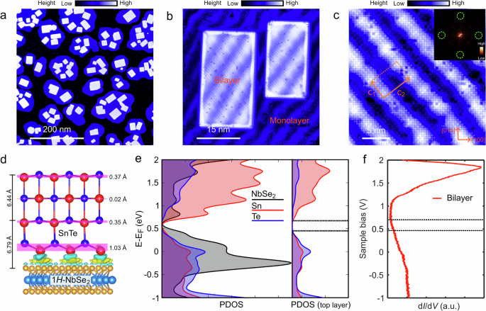
a Large-scale STM topographic image of bilayer SnTe on the 2H-NbSe2 substrate (tunneling parameters: Vb=1 V, I=2.5 pA). b Typical STM image of bilayer SnTe islands with visible stripe patterns (Vb=0.8 V, I=200 pA). c Atomic-resolution STM topography of bilayer SnTe islands (Vb=0.3 V, I=230 pA). Sublattice Sn atoms are aligned along [100] and [010] directions indicated by orange color, which corresponds to a set of Bragg lattice peaks outlined by green dashed circles in the FFT image shown in the inset. One of strain superlattice unit cells is marked by a nearly rectangular frame along c1 and c2 directions. d Side view of the heterostructure model of 4-AL SnTe on 1H-NbSe2 after full relaxation. The charge difference at the interface shown by green and yellow colors reveals that the bottom 1-AL SnTe bonds to the 1H-NbSe2 underneath through Sn atoms, giving rise to its substantial decoupling from the top 3 ALs. The red, dark blue, orange, and light blue balls represent Sn, Te, Se and Nb atoms, respectively. e Calculated PDOS of bilayer SnTe/1H-NbSe2 by DFT methods. The left panel shows the PDOS components of all the Sn, Te and NbSe2 orbitals onto themselves while the right panel displays PDOS of all the Sn and Te orbitals onto the Sn and Te atoms of the topmost atomic layer. f Tunneling differential spectrum taken in the middle of bilayer SnTe. Two pairs of horizontal black dashed lines in e and f indicate the calculated and experimental bulk band gap edges of bilayer SnTe.
To gain further insight into the structural and electronic properties of this strained system, particularly for the 4-AL SnTe/2H-NbSe2 heterostructure, we performed DFT calculations based on the experimentally extracted lattice parameters. Figure 1d presents the side view of our heterostructure model after full relaxation (see also Supplementary Information Fig. S8). The calculations reveal that the metallic NbSe2 substrate provides a high density of states near the Fermi level, facilitating charge transfer and inducing p-type doping into the SnTe due to the alignment of the Fermi level. The charge transfer induces strong hybridization between the orbitals of the SnTe bottom layer and the underlying 1H-NbSe2, causing the Sn atoms in the bottommost AL to bond directly with the substrate. Due to the substantial lattice mismatch, the upper 3 ALs become structurally decoupled from the wetting layer, exhibiting noticeable distortion. The computed interlayer distances are consistent with the experimental height profile (Supplementary Information Fig. S9). The projected density of states (PDOS) for the topmost AL, shown in Fig. 1e, aligns well with the experimental tunneling spectra (Fig. 1f), where the bulk band gap edges are marked by black dashed lines. Further, the layer-wise PDOS (shown in Supplementary Information Fig. S9d) suggests that the PDOS in the bottom layer bonded to the substrate is quite different from the remaining 3 ALs. In addition to charge transfer from the substrate, Sn vacancies estimated at a surface density of 1013 cm−2 further promote p-type doping, shifting the Fermi level below the valence band maximum31. The bilayer bulk gap, determined from negative differential resistance measurements, ranges from 0.2 to 0.3 eV (see Supplementary Information Fig. S15). Together, these findings indicate that the experimental system effectively realizes a strained 3-AL SnTe structure on top of a 1-AL wetting layer, stabilized on the 2H-NbSe2 substrate. This interpretation, supported by both structural and spectroscopic evidence, provides a solid foundation for theoretical investigation into the topological properties of this system.
Lifshitz transition driven by biaxial strain
Building on this understanding, we now focus on the theoretical analysis of the topological characteristics of the strained 3-AL SnTe structure, using parameters fitted from the DFT-calculated configuration where the bottom 1-AL SnTe is bonded to the substrate. To ensure the robustness of our theoretical model and its relevance to the experimentally realized structure, we also analyze the general behavior of few-layer SnTe systems (see Supplementary Information Figs. S1 and S2). As shown in Fig. 2a, a 3-AL SnTe structural model has a cubic rock-salt structure with a Sn-Sn spacing of 4.5 Å and preserves the reflection symmetry z → − z with respect to the atomic layer in the middle plane (pink shadow). This system hosts two equivalent high-symmetry X points in the 2D Brillouin zone. On the other hand, ultrathin SnTe films are known to spontaneously distort along the {110} direction into a parallelogram structure and form a ferroelectric phase27. This in-plane 2D ferroelectricity does not break the vertical mirror symmetry. This allows for competition between ferroelectricity and a TCI phase. Ab initio calculations enable us to establish a phase diagram of the 3-AL SnTe system as a function of biaxial strain. Figure 2b shows ferroelectric displacement δFE of this system evolves with the lattice parameter. Above the critical value of a ≃ 4.38 Å, the phonon instability associated with the ferroelectric distortion appears (see Supplementary Information Fig. S5) as the lattice parameters expand. Meanwhile, this system opens a band gap at the X point. These findings indicate ferroelectric order occurs in the xy plane of biaxially tensile 3-AL system. When the lattice parameters reduce to the critical value, the band gap closes. Below the critical value, the band gap reopens, as shown in Fig. 2d. This change in Fermi surface topology corresponds to a Lifshitz transition driven by the change from the tensile to compressive strain. The gap closing at the X point is the critical point of a phase transition (Fig. 2c), where biaxial compressive strain and spin-orbit coupling can induce a band inversion from Sn and Te orbitals (see Supplementary Information Fig. S3). The electronic structure induces the stabilization of the high-symmetry crystalline phase, quenching the ferroelectric displacement. We further experimentally exclude the possibility of ferroelectricity in our compressive system by probing band bending of conduction band at the edges (shown in Supplementary Information Fig. S22).
Fig. 2: Crystal structure and band structure of 3-AL SnTe.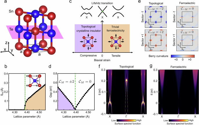
a Schematic structure of 3-AL SnTe along the (001) orientation, where one mirror plane in the middle of this system from z → − z is indicated by a pink shadow. b Ferroelectric displacement δFE between the cation Sn and anion Te evolves with in-plane lattice parameter, schematically represented at the right-top corner. c Phase diagram of a 3-AL SnTe system as a function of biaxial strain. A Lifshitz transition at the X point takes place when strain goes through from tensile to compressive regime. Correspondingly, the change in Fermi surface topology produces trivial ferroelectric order in tension and a TCI phase in compression. d Evolution of the band gap at the X point with the lattice constant. The closing of the band gap triggers a topological phase transition that can be defined by time-reversal-mirror Chern number \({{{{\mathcal{C}}}}}_{M}\). e Left(right) plots demonstrate the mirror Berry curvature in reciprocal space for a topological (ferroelectric) phase for the -1 (top) and +1 (bottom) mirror sectors, respectively. f–g, Band structure along X-Γ-X direction for the topological (ferroelectric) phase of a semi-infinite ribbon calculated with the lattice parameter of 4.33 Å (4.51 Å). Two Dirac points are visible at the X and Γ points for the topological phase.
The topological invariant of a strained 3-AL SnTe system can be obtained in the gapped phases by extracting a Wannier Hamiltonian from DFT calculations. The results show that the time-reversal-mirror Chern number vanishes \({{{{\mathcal{C}}}}}_{\pm M}=0\) in the tensile regime while the time-reversal-mirror Chern number is \({{{{\mathcal{C}}}}}_{\pm M}=\pm 2\) in the compressive regime (Fig. 2d), signaling the emergence of a TCI phase. This finding is schematically depicted in Fig. 2c. Figure 2e displays the computed time-reversal-mirror Berry curvature for each of the symmetry sectors ( ± 1) of the operator \({{{\mathcal{M}}}}={M}_{(001)}\Theta\), where M(001) is the (001) mirror and Θ is the time-reversal symmetry operator. In the topological phase, the mirror Berry curvature is well localized around two X points and possesses an opposite sign for each symmetry sector. In the ferroelectric phase, the mirror Berry curvature is not localized and changes the sign with each symmetry sector, resulting in \({{{{\mathcal{C}}}}}_{\pm M}=0\). The bulk-boundary correspondence requires that there must be gapless edge states in the biaxially compressive 3-AL system. The time-reversal-mirror Chern number of ± 2 allows two pairs of Dirac cones located around X points in the 2D Brillouin zone, and with further projection into the specific edges, we obtain two pairs of edge state subbands along the X-Γ-X direction (Fig. 2f). Co-propagating edge states carry identical mirror eigenvalues. At the band crossings at Γ and X points, edge states with opposite mirror eigenvalues propagate in the opposite direction. The two pairs of edge state subbands exhibit linear dispersion around the crossing points, extending into the bulk band gap. In contrast, there are no gapless edge states connecting valence and conduction bands in the ferroelectric phase, as shown in Fig. 2g. Although we used slightly different lattice parameters compared to the experimental values, the essential conclusions remain unchanged: while the band gap size can be tuned by lattice parameters, the two phases preserve their respective band structures and topological characteristics.
Experimental evidence of topological edge states
We present two direct experimental proofs to verify the existence of a 2D TCI in our effective 3-AL system. The first one is that we observe two strong peaks associated to two pairs of edge states extending to the bulk gap along the specific edges of bilayer SnTe islands. As shown in Fig. 3a, the dI/dV spectrum taken at the bilayer edge exhibits two pronounced peaks located around 0.5 V (peak 1) and 1.55 V (peak 2). We attribute these peaks to edge states (see Supplementary Information Figs. S10 and S11). These experimental results can be compared with calculations by computing the density of states (DOS) in the bulk and edge of the compressive 3-AL system, where we obtain two sharp peaks with one residing in the bulk gap and the other within the conduction band of bulk states. The low-energy (high-energy) peak at the edge is produced by the substantially enhanced DOS induced by the flatter dispersion of the pair of edge states at the X (Γ) crossing point (Fig. 2f). Therefore, each peak corresponds to the crossing of counter-propagating pairs of edge states. The edge state subbands above the peak 1 are fully within the bulk gap (from 0.5 to 0.7 eV) and are also spatially localized (see Supplementary Information Fig. S12). The discrepancy of the energy peak positions between theory and experiment stems from the typical underestimation of the band gap in DFT calculations.
Fig. 3: The topological edge states and their spatial variation.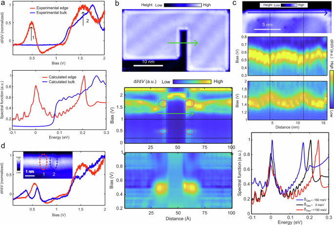
a Tunneling differential spectra taken in the middle and edge of bilayer SnTe on the 2H-NbSe2 (top panel) and calculated spectral function of the bulk and edge in the compressively strained 3-AL system (bottom panel). The spectral function is calculated by integrating all the subbands shown in Fig. 2f for a given energy. b Plots of dI/dVspectra in different energy ranges along the linecut (top panel) are shown in the middle and bottom panel(Vb =1 V, I=2 pA). Two pairs of edge state peaks are highlighted by red dashed oval frames. c Two edge state peaks vary periodically with strained moiré patterns at the edge of bilayer SnTe islands (top and middle panel)(Vb=0.8 V, I=2.2 pA). They have a π phase difference in spatial variation. We used a phenomenological method to reproduce this result by calculations (bottom panel). δGap represents the energy gap between two edge state peaks. d Tunneling spectra taken at the edges without (with) typical atomic defects of bilayer islands, where the positions of the spectra are indicated by red and blue ovals (Vb=0.8 V, I=5 pA).
To resolve the spatial modulation of edge states, we first conduct dI/dV spectroscopy across the opposite edges of a bilayer island (top panel in Fig. 3b). At each edge, there are two edge state peaks located at low and high energies, outlined by the dashed oval frames in the middle panel. These peaks are highly localized around the edges. Similar to the observations in Fig. 3a, the peak 1 almost resides the bulk gap (bottom panel) while the peak 2 lies inside the conduction band. It is important to note that the exact energy position of the edge states depends on the strain field, e.g., the strain field can shift the energy of the peak 1 beyond the bulk gap. Series of local DOS (LDOS) oscillations between 0.2 and 1 V as shown in the bottom panel of Fig. 3b are likely to be related to the LDOS oscillations in the SnTe wetting layer (see further details in the Supplementary Information Fig. S14). We also performed dI/dV spectroscopy along the blue linecut indicated in Fig. 3c (top panel). The results show that both peak 1 and peak 2 modulate periodically with the moiré pattern at the island edges (two middle panels). FFT analysis further reveals that the edge-state crossings occur at low energy near the X point and at higher energy near Γ (see Supplementary Information Fig. S13) in agreement with the theoretical prediction shown in Fig. 2f. The detailed dispersions of these edge-state crossings are difficult to extract experimentally due to resolution limitations. Interestingly, the two peaks are anticorrelated, exhibiting a π phase difference. The energy shift of the peak 2 is approximately 2 times as large as the peak 1. To rationalize these observations, we developed a phenomenological model. Considering that strain induces changes in the band gap (Fig. 2d), by renormalizing the energy gap as dictated by the strain modulation, we account for the impact of the strain field on the energy position of each pair of edge states. As shown in the bottom panel, our calculations reproduces the experimental results. Moreover, dI/dV maps at different energies (see Supplementary Information Fig. S18) reveal that the two pairs of edge states span the bulk energy gap along the perimeters of bilayer islands at 0.5 and 0.6 V. They only emerge along the sharp and straight edges with specific atomic terminations of either Sn or Te atoms, a characteristic observed in both regular and irregular bilayer SnTe structures (see Supplementary Information Figs. S4, S19 ~ S21).
Since the edge states in our system are protected by time-reversal-mirror symmetry, the second piece of evidence to confirm a 2D TCI is to observe a band gap in the edge states when time-reversal-mirror symmetry is broken. Time-reversal-mirror symmetry can be disrupted spontaneously or through external perturbations such as perpendicular electric field or an in-plane magnetic field23. In contrast with time-reversal symmetry, disorder can always break time-reversal-mirror symmetry. In our effective 3-AL system, intrinsic atomic defects at the edges locally and randomly break the z → − z mirror symmetry about the middle plane. As a result, the edge states open up a band gap, as shown in Fig. 3d. This is supported by theoretical simulations (see Supplementary Information Fig. S16). The depth of the opened band gap depends on the extent to which mirror symmetry is broken at the edges. Remarkably, we find that the edge states are substantially resilient to the effects of the substrate, the moiré potential, and even a sizable electric field (see Supplementary Information Figs. S16 and S17).
The link between theory and experiment can be further strengthened by investigating the strain-driven transition between the topological and trivial phases. We have achieved precise control over the in-plane lattice constants of the bilayer SnTe by tuning the growth parameters. This tunability allows us to modulate the system across the topological phase boundary. When the lattice constants are smaller than the critical value identified in Fig. 2d-i.e., in the compressively strained regime-the bilayer SnTe islands consistently exhibit robust topological edge states. In contrast, when the lattice constants exceed this critical value, entering the tensile strain regime, the edge states vanish along all observed edges. Details are shown in Supplementary Information Figs. S23–S25. This experimental observation directly supports the strain-driven topological phase transition predicted by theory and further validates the topological nature of the observed edge states in our system.
Coupling of topological edge states
The interaction of edge states in 3D TCIs has been studied26,32. We probe the possibility of observing coupling between the edge states in our 2D TCI by examining two closely adjacent bilayer islands, as illustrated in Fig. 4a. High-resolution topography indicates no significant structural distortions or atomic defects that could disrupt mirror symmetry; therefore, a gap opening in the edge states is not expected. To eliminate the influence of strain, which can shift edge state energy, the tunneling spectra were taken at equivalent points on the same stripe pattern, ensuring a consistent strain field. Our dI/dV spectra reveal that peak 1 shifts to lower energy compared to isolated edges as indicated by the black arrow (Fig. 4b) and its intensity weakens significantly around 0.6 V. The energy shift due to the proximity of adjacent edges exhibits an exponential decay with increasing distance between the two edges, as seen in Fig. 4c, with a decay length of approximately 5 nm. This effect is most evident in the dI/dV mapping over the bilayer edges at different energies (Fig. 4d–g), as outlined by the orange and red rectangular frames.
Fig. 4: Coupling of topological edge channels.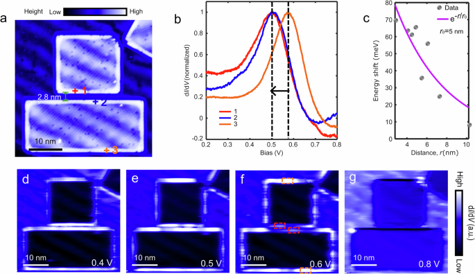
a STM topographic image of two adjacent bilayer SnTe islands (Vb=0.5 V, I=60 pA). The distance of their neighboring edges is 2.8 nm. b Tunneling spectra taken at the equivalent points 1, 2 and 3 from three edges in a by locating the local maximum position of the edge state peaks. The black arrow indicates the shift direction of neighboring edge states. c The blue curve fits the exponential decay of the energy shift of edge states with the increasing distance between two adjacent edges. The decay length is 5 nm. d–g dI/dV maps over the bilayer island from a at different bias voltages. The red and orange dashed rectangular frames outline the edge states with and without neighboring edges. The tunnel junction setup is Iset=60 pA.
We propose two possible origins for the observed energy shift, both of which are expected to coexist in our system. First, we experimentally find that the edge states shift to lower energies compared to isolated edges. This behavior can be explained by electrostatic coupling: the presence of adjacent edges leads to interactions that modify the energy position of the edge states. The strength of this coupling depends on both the edge-to-edge separation and the local charge distribution. Importantly, this charge redistribution stems from edge reconstruction, a phenomenon that becomes particularly pronounced in materials that lie close to an electronic phase transition, where small structural changes can strongly affect the electronic configuration.
Second, there is a possibility of substrate-mediated tunneling between adjacent edges, allowing for interaction through proximity. To assess the magnitude of this effect, we developed a model where the electronic modes in one bilayer island can tunnel into another island through an effective barrier potential V (details in Supplementary Information Fig. S26). This tunneling coupling leads to a shift of the crossing Dirac point. Comparison with the experimental results is possible by relating V to the distance d between neighboring edges through \(\lambda d=ln(\frac{V}{{t}_{0}})\), where t0 is the hopping energy of SnTe orbitals (on the order of eV) and λ is a finite phenomenological parameter that can be adjusted based on experimental data. This model results in an exponential decay of the energy shift as λd increases, consistent with our experimental results. In summary, it is likely that a combination of electrostatic interactions and tunneling coupling is responsible for the energy shift of edge modes for closely spaced SnTe edges.