
Materials
Urea, potassium chloride (KCl, 99.999%), thioglycolic acid, hydrochloric acid (HCl, 37%), N,N-dimethylformamide (DMF, 99.8%), dimethyl sulfoxide (DMSO, ≥99.9%), acetonitrile (ACN, 99.8%), chlorobenzene (CB, 99.8%), bis(trifluoromethane)sulfonimide lithium salt (Li-TFSI, 99.95%), 4-tert-butylpyridine (98%), zinc oxide (ZnO), tin(II) iodide (SnI2), tin(II) fluoride (SnF2), bathocuproine, glycine hydrochloride, C60, [6,6]-phenyl-C61-butyric acid methyl ester (PCBM) and nanoparticle ink solution were purchased from Sigma Aldrich. FA iodide (>99.99%), methylammonium iodide, methylammonium chloride (MACl, >99.99%) and n-octylammonium iodide (>99%) were purchased from Greatcell solar. 2,2′,7,7′-tetrakis[N,N-di(4-methoxyphenyl)amino]-9,9′-spirobifluorene (spiro-OMeTAD) and tris(2-(1H-pyrazol-1-yl)-4-tert-butylpyridine)cobalt(III) tri[bis(trifluoromethane)]sulfonamide (FK209) were purchased from Lumtec. Lead(II) iodide (99.99%), [4-(3,6-dimethyl-9H-carbazol-9-yl)butyl]phosphonic acid (Me-4PACz), ethane-1,2-diammonium iodide (EDAI2) and guanidine thiocyanate (GuaSCN) were purchased from the Tokyo Chemical Industry. SnCl2·2H2O, 2-methoxyethanol (2-Me, 99%+) was purchased from Alfa Aesar. Diethyl ether (99.5%) was purchased from SAMCHUN. Poly(3,4-ethylenedioxythiophene) polystyrene sulfonate (PEDOT:PSS; Al 4083) were purchased from Ossila.
FAPbI3 micro powder synthesis
The black-phase FAPbI3 micro powder was synthesized in accordance with previously published protocols4,47. Specifically, the micro powder was synthesized by using 0.8 M precursor solution containing FA iodide and PbI2 in 33 ml of 2-Me. The precursor solution with stirring bar was heated to 120 °C in an oil bath and then precipitated using the retrograde method for 3 h. The filtered FAPbI3 micro powder was baked at 150 °C for 30 min.
C8N1 2D micro powder synthesis
A mixed solution of HI solution (16 ml) and H3PO2 solution (2 ml) was prepared in a 200-ml glass volumetric flask. PbO powder (2,232 mg, 10 mmol) was dissolved by heating to boiling under stirring, and it formed a bright yellow solution; 1,669 μl (10 mmol) of octylamine was then added to this solution and stirring was discontinued. The temperature was lowered to 80 °C over 30 min. The solution was left at room temperature until orange crystals began to form. The crystals were isolated by suction filtration and thoroughly dried in a vacuum chamber.
2D perovskite thin film fabrication
ITO substrates of 2.5 cm × 2.5 cm were sequentially washed with deionized water, acetone, and 2-propanol for 15 min each. The substrates were then cleaned with UV/O3 for 15 min for better wetting of the 2D perovskite precursor solution. 0.2 M (R)2PbI4 (where R is C4, C8, or C12) precursor solution was prepared by dissolving in DMSO and DMF with a volume ratio of 1:8. The precursor solution was then spin-coated on the substrate at 5,000 rpm (acceleration 5,000 rpm s−1) for 20 s; 1 ml of diethyl ether was quickly poured onto the substrate at 10 s. Then, the 2D perovskite film was transferred to a hot plate and heat-treated at 80 °C for 5 min. For the PbSn devices, an EDAPbI4 precursor solution with a concentration of 0.2 M was prepared by dissolving EDAI2 and PbI2 in a 1:1 molar ratio in a mixed solvent of DMF and DMSO (8:1, v/v). The precursor was then spin-coated onto ITO substrates at 6,000 rpm (acceleration 6,000 rpm s−1) for 30 s, and 1 ml of diethyl ether was quickly dripped onto the substrate 10 s before the end of the spin-coating step. The films were subsequently annealed at 100 °C for 5 min. We recommend that the 2D perovskite film be produced at 30–40% relative humidity.
Electron transport layer fabrication for n–i–p architecture device
Prepatterned Ashahi FTO substrates were cleaned with deionized water, acetone, ethanol and 2-propanol for 15 min, respectively. The substrates were then treated with UV/O3 for 30 min before tin oxide (SnO2) deposition. 10 mM of SnCl2·2H2O with 10 g of urea was dissolved in 200 μl of thioglycolic acid, 10 ml of HCl and 800 ml of deionized water. FTO substrate was dipped in the solution at 90 °C for 6 h according to previous reports2,48. The substrates for depositing SnO2 were then heat-treated at 150 °C for 6 h.
Hole transport layer fabrication for p–i–n device
Prepatterned Ashahi FTO substrates were cleaned with deionized water, acetone, ethanol and 2-propanol for 15 min, respectively. The substrates were then treated with UV/O3 for 60 min. A total of 0.1 ml of Me-4PACz solution (0.4 mg ml−1 in ethanol) was loaded onto the substrate and coated at 3,000 rpm (acceleration 3,000 rpm s−1) for 30 s. Then, the Me-4PACz coated substrate was heat-treated at 120 °C for 10 min. This process was repeated twice to ensure device reproducibility. For the PbSn devices, PEDOT:PSS diluted with deionized water at a 1:4 volume ratio was spin-coated onto FTO substrates at 6,000 rpm for 40 s, followed by thermal annealing at 120 °C for 20 min. The substrates were then immediately transferred to a nitrogen-filled glovebox after annealing.
3D thin film fabrication for n–i–p device
The FTO/SnO2 substrates were cleaned by UV–ozone for a further 15 min. KCl solution (30 mM KCl in deionized water) was spin-coated on the FTO/SnO2 substrate at 5,000 rpm (acceleration 2,500 rpm s−1) for 30 s. Then, the substrate was annealed at 150 °C for 10 min. A total of 1.8 M perovskite precursor solution with the composition of FAPbI3 was prepared by dissolving 1.317 g (2.08 mmol) of FAPbI3 and 0.0492 g (0.728 mmol) of MACl in 1.01 ml (0.951 g) of DMF and 0.15 ml (0.1625 g, 2.08 mmol) of DMSO. Then, 70 μl of the precursor solution was dropped and spin-coated on the FTO/SnO2 substrate through a two-step spin-coating procedure with 1,000 rpm (acceleration 1,000 rpm s−1) for 5 s and 5,000 rpm (acceleration 1,000 rpm s−1) for 10 s. A total of 1 ml of diethyl ether was quickly poured on the substrate 1 s before the second step end. The yellow film was quickly transferred to a hot plate and annealed at 120 °C for 100 min.
3D thin film fabrication for p–i–n device
Al2O3 dispersion solution (0.2 wt%) was spin-coated on the FTO/Me-4PACz substrate at 3,000 rpm for 30 s. Then, the substrate was annealed at 120 °C for 5 min. A total of 1.8 M perovskite precursor solution with the composition of FAPbI3 was prepared by dissolving 1.317 g (2.08 mmol) of FAPbI3 and 0.0421 g (0.624 mmol) of MACl in 1.01 ml (0.951 g) of DMF and 0.15 ml (0.1625 g, 2.08 mmol) of DMSO. Then, 70 μl of the precursor solution was dropped and spin-coated on the FTO/Me-4PACz substrate through a two-step spin-coating procedure with 1,000 rpm (acceleration 1,000 rpm s−1) for 5 s and 5,000 rpm (acceleration 1,000 rpm s−1) for 10 s. A total of 0.1 ml of CB was quickly poured on the substrate 1 s before the second step end. The yellow film was quickly transferred to a hot plate and annealed at 120 °C for 100 min. For the PbSn device, a 2.2-M [FASnI3]0.6[MAPbI3]0.4 precursor solution was prepared in a mixed solvent of DMF and DMSO with a 4:1 volume ratio. SnF2 (5 mol% with respect to SnI2), GuaSCN (7 mol% with respect to methylammonium iodide) and glycine hydrochloride (2 mol% with respect to the total Sn and Pb) were added as additives, and the solution was stirred at room temperature for 2 h. The PbSn perovskite films were then deposited on PEDOT:PSS-coated substrates by spin-coating at 1,000 rpm for 10 s and 4,000 rpm for 30 s, during which 0.5 ml of toluene was dripped onto the substrate 20 s before the end of the second step. The resulting perovskite films were annealed at 100 °C for 10 min.
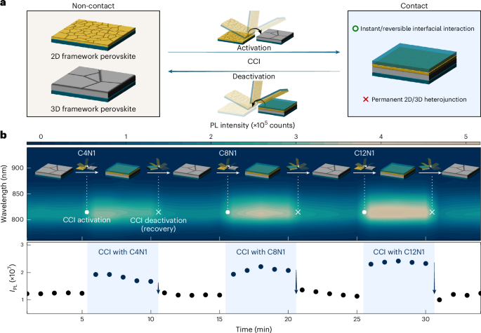
Fabrication of CCI-driven 3D perovskite
The previously fabricated C8N1 or C12N1 thin film was placed on the 3D perovskite thin film so that the two surfaces were in contact. The stacked films were moved on the hot plate to supply heat towards the 2D direction, and then the balance weight (100 g) was placed on the stacked films. For CCI-driven 3D PbSn perovskite, the 2D perovskite was replaced with EDAPbI4, and the same procedure was conducted in a nitrogen-filled glovebox.
Hole transport layer and counter electrode fabrication for n–i–p device
The Spiro-OMeTAD solution was prepared by adding 23 μl of Li-TFSI solution (540 mg ml−1 in ACN), 10 μl of FK209 solution (376 mg ml−1 in ACN) and 39 μl of 4-tert-butylpyridine to 100 mg of spiro-OMeTAD in 1.1 ml of CB. The Spiro-OMeTAD was deposited by dynamic spin coating on the FAPbI3 and CCI-driven FAPbI3 at 2,000 rpm for 30 s. Finally, the gold electrode was deposited by thermal evaporation. The deposition area of the counter electrode was fixed at 0.16 cm2.
Electron transport layer and counter electrode fabrication for p–i–n device
The C60/ZnO bilayer was used as the electron transport layer in the inverted structure46. First, a 20-nm-thick layer of C60 was formed by thermal evaporation. For ZnO layer, ZnO nanoparticle ink was diluted with 2-propanol, coated at 3,000 rpm for 30 s and annealed at 80 °C for 5 min. Finally, the silver electrode was deposited by thermal evaporation. In the PbSn device fabrication, a PCBM solution (7.5 mg ml−1) was deposited onto the PbSn perovskite layer by spin-coating at 5,000 rpm for 50 s and then annealed at 100 °C for 5 min. After the substrates were cooled to room temperature, C60 (15 nm) and bathocuproine (8 nm) layers were sequentially formed by thermal evaporation at 0.1–0.3 Å s−1. Finally, a 130-nm Cu electrode was thermally evaporated at a deposition rate of 3.0 Å s−1. The deposition area of the counter electrode was fixed at 0.16 cm2.
Characterization
The film morphologies were obtained by using a field-emission scanning electron microscope (Hitachi, S-4800). XRD was performed using a Rigaku SmartLab X-ray diffractometer with an X-ray tube (copper Kα, λ = 1.54 Å, 200 mA, 45 kV, 9 kW) at the National Center for Inter-university Research Facilities at Seoul National University. All XRD curves were measured under a scan rate 1° per minute with a step of 0.02°. Standard material (LaB6) was performed to confirm the instrument broadening. The values of full width at half-maximum were adjusted by using the instrumental broadening according to the previous report49. The optical absorbance properties of the films were measured using UV–Vis–near-infrared spectrophotometer (Agilent, Cary 5000). To obtain the J–V PCE, the devices were measured using a solar simulator (Newport, 94043A) with a source meter (Keithley 2400). The light intensity with AM1.5G illumination was adjusted using a calibrated reference cell (Newport, KG with quartz and KG3). J–V PCEs were measured from −0.2 V to 1.2 V at 100 mV s−1 and 10-mV step intervals. All devices were covered with a metal mask, fixing the active area to 0.096 cm². External quantum efficiencies were measured from 320 nm to 900 nm at 10-nm intervals (Newport, QuantX-300). Stabilized power outputs were obtained using a potentiostat (IviumStat.h).
Computational method
The DFT calculations were performed using the VASP code with projector augmented-wave pseudopotentials50,51. A plane-wave cutoff of 600 eV and a 3 × 3 × 1 k-point mesh were adopted. The Perdew–Burke–Ernzerhof functional was used to describe exchange–correlation interactions52, whereas van der Waals forces were accounted for using Grimme’s D3 correction53. All residual atomic forces were converged to below 0.02 eV Å−1 during structural relaxation. The 3D crystal structure of the perovskite was visualized using the VESTA software54.
Grazing-incidence wide-angle X-ray scattering measurement
The grazing-incidence XRD measurements were conducted at the PLS-II 6D beamline of Pohang Accelerator Laboratory in Korea. The X-rays emitted from the bending magnet were monochromatized to 18.986 keV (λ = 0.6530 Å) using a double-crystal monochromator and focused both vertically and horizontally using a sagittal Si(111) crystal and toroidal mirror. The grazing-incidence wide-angle XRD patterns were recorded with a 2D X-ray charge-coupled device detector (MX 225-HS, Rayonix). The incidence angles of 0.117°, 0.145°, 0.3°, 0.483° and 0.8° were used for investigating the penetration depth dependency of perovskite films. The diffraction angles were calibrated using LaB6 (standard reference material 660c, National Institute of Standards and Technology), and the sample-to-detector distance was ~240 mm. The 2D grazing-incidence wide-angle XRD images were converted to one-dimensional qx or qz profiles using a MATLAB-based homemade program.
PiFM measurements
PiFM data were obtained under ambient conditions using a VistaScope AFM platform, manufactured by Molecular Vista, exploiting a QCL laser (760–1,860 cm−1). The technique provides simultaneous topographic and vibrational spectroscopy information. In the experiments reported here, the sample was mapped at 1,711 cm−1 characteristic of the C=N stretching band of the FA ion. The ‘bulk’ region was scanned with direct detection mode which samples a depth of up to ~300 nm, where the cantilever is actuated at its primary resonance frequency v1, whereas the repetition rate of the stimulating laser is adjusted to correspond to the secondary resonance frequency v2. The ‘surface’ region was scanned using sideband mode detection which samples a depth of ~20–30 nm, wherein the second driving force is modulated to a ‘beat’ frequency, which corresponds to the difference or sum of the two mechanical resonances as v1 − v2 (or v1 + v2).
Absolute PLQE measurement
The PLQE and PL spectrum were obtained a 3.2-inch integrating sphere (Horiba, FL-sphere), a fluorometer (Horiba, Fluorolog-3), continuous wave mode of diode laser with 485 nm (Horiba, DeltaDiode-485L-CW) at a continuous power density of 73 mWcm−2 (excitation density of 1.8 × 1018 cm−3). The focus area of the laser was confirmed using a laser beam profiler (Newport, LBP2-HR-VIS3). The emission light was collected with a double grating monochromator (Horiba, FL-1005) and a liquid-nitrogen-cooled low-noise photomultiplier tube (Hamamatsu, R5509-43). The absolute PLQE was calculated through the PL spectrum under three conditions: (1) reference laser intensity condition, (2) indirect excitation condition and (3) direct excitation condition55.
Time-resolved PL measurement
PL decays were obtained time-correlated single-photon-counting method using the double grating monochromator (Horiba, FL-1005) and the liquid-nitrogen-cooled low-noise photomultiplier tube (Hamamatsu, R5509-43). To excite the perovskite film, the pulsed mode of a diode laser with 485 nm (Horiba, DeltaDiode-485L-CW) was used at a fluence of 1.49 nJ cm−2 and a repetition rate of 62.5 kHz.
PHEM
The photo-Hall effect measurement (PHEM) specimens were prepared using a prepatterned ITO substrate according to the previous report56. All specimens were encapsulated with edge sealing type using 1.1 mm glass and UV-curing resin (Three Bond, 3052B), which was cured under a UV lamp with peak emission at 365 nm (KJUV, KJUV-HS-05). PHEM was measured using a customized PHEM system, which consists of a Hall effect measurement system (ECOPIA, HS7000) with a magnet kit (353 T), 100 W LED with 465 nm and source meter unit (Keithley 2450). An optical power meter (Newport, 1919-R) was used to calculate the absorbed photon density at each light intensity. To control the change of light intensity, the temperature of the LED was maintained through a thermoelectric device. At every light intensity, voltage signals were measured, and then photoconductivity and Hall coefficient were calculated using van der Pauw method. To obtain transport parameters of each carrier, carrier-resolved photo-Hall effect analysis was used, and the final transport parameters were extracted from initial transport parameters using a generalized \(\triangle \mu\) model57,58. The mobility values were obtained by fitting the experimental data according to established models, assuming constant mobility for holes and electrons in Fig. 4e, following precedent in the literature57.
Electroluminescence quantum efficient measurement
The electroluminescence spectrum was obtained using the double grating monochromator (Horiba, FL-1005), the liquid-nitrogen-cooled low-noise photomultiplier tube (Hamamatsu, R5509-43), the 3.2-inch integrating sphere (Horiba, FL-sphere) and the source meter unit (Keithley 2450) under injection current density, which corresponded to extracted from the device in the standard test condition. Electroluminescence quantum efficients were measured by directly attaching a calibrated silicon photodiode (Hamamatsu, S1227-1010BQ), which was large collection area than the active area of device. The inject current of the source meter unit (Keithley 2450) and the detected photocurrent of the photodiode were controlled and measured using the software ‘SweepMe!’59.
Device stability test measurement
For the operating test, all devices were encapsulated using 1.1-mm cover glass, polyisobutylene (PIB) tape and UV-curing resin (Three Bond, 3052B). First, the corners of the device, which does not operate as the solar cell, were removed with 2-Me. PIB tape was placed between the device and the cover glass, and the pressure was applied to proceed with the primary encapsulation. Second, edges of device were covered with the resin. The operational tests were performed using a self-customized system and LED solar simulator (Newport, LSH-7320). MPPT was measured using a source meter (Keithley 2450). Every hour, the current from the maximum power point was tracked. The thermal stress under illumination test was performed using device on a hot plate for heat supply.
Reporting summary
Further information on research design is available in the Nature Portfolio Reporting Summary linked to this article.