
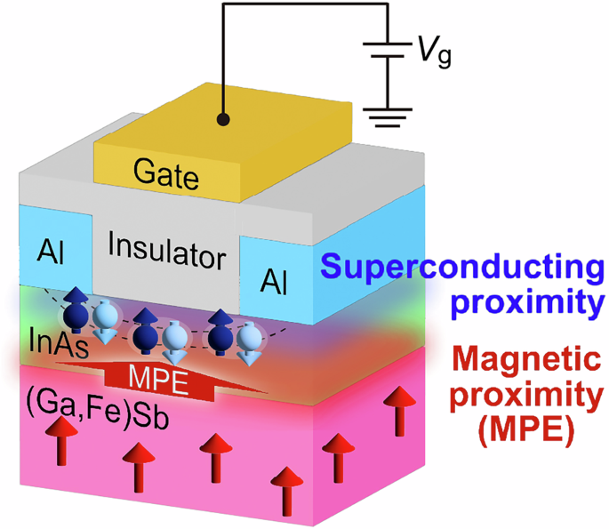
The Al/InAs/(Ga,Fe)Sb heterostructure grown by low-temperature molecular beam epitaxy (LT-MBE) is shown in Fig. 2a. After growing AlSb/AlAs buffer layers on a GaAs (001) semi-insulating substrate, a 5 nm-thick (In,Ga)As/15 nm-thick InAs/20 nm-thick (Ga,Fe)Sb heterostructure, from top to bottom, was grown at 250 °C to suppress Fe segregation in the (Ga,Fe)Sb layer. The thin (In,Ga)As layer containing 19% indium (In) is inserted between the Al and the InAs layers to make better superconductor/semiconductor interfaces. This follows previous epitaxial Al/InAs platforms in which an (In,Ga)As cap layer was used to obtain an atomically abrupt Al/semiconductor interface while maintaining the electronic properties of the InAs quantum well21,26,30,31. The (Ga,Fe)Sb layer containing 14.6% iron (Fe) is an FMS layer to induce a magnetic proximity effect in the adjacent InAs layer. A 26 nm-thick Al film was subsequently grown in situ at a temperature below −40 °C. Transmission electron microscopy (TEM) images in Fig. 2b, c show that the semiconductor layers retain the zinc-blende-type crystal structure throughout MBE growth. Although local disorders or defects are observed in the thin (In,Ga)As layer, it still serves its intended role in forming a sufficiently transparent superconductor/semiconductor interface, as supported by the results discussed below. Figure 2c further indicates that the Al film grows along the [111] direction of the face-centered cubic crystal, consistent with the X-ray diffraction results presented in Supplementary Material. The TEM analysis also confirms that the Al/(In,Ga)As interface is clean and atomically sharp.
Fig. 2: Structural, electrical transport, and magnetic characterizations of the Al/InAs/(Ga,Fe)Sb heterostructure.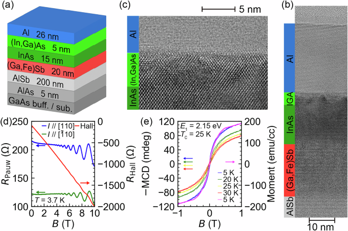
a Schematic structure of the sample used in this study. b, c Cross-sectional transmission electron microscopy lattice images of the Al / (In,Ga)As / InAs / FMS (Ga,Fe)Sb heterostructure with the incident direction along the [110] axis of the GaAs (001) substrate. The semiconductor layers are grown in the (001) orientation with a zinc-blende-type crystal structure, while the Al layer is grown in the (111) orientation with a face-centered cubic crystal structure. d Magnetotransport of the InAs channel under a perpendicular magnetic field at 3.7 K. The resistance of InAs was measured by the Van der Pauw method using a cleaved 5 × 5 mm2 piece. Blue and green curves represent the resistance with current applied along the [110] and [\(\bar{1}\)10] crystal axes, respectively, while the red curve shows the Hall resistance. e Magnetic properties of the (Ga,Fe)Sb layer obtained by MCD and SQUID measurements. MCD measurements were performed at the critical point energy E1 = 2.15 eV of GaSb. MCD and SQUID results show good agreement at 5 K.
We first characterise the sample transport and magnetic properties. Magnetotransport of the InAs layer at 3.7 K under a perpendicular magnetic field was measured after removing the Al layer by wet etching. As shown in Fig. 2d, we observe clear Shubnikov-de Haas (SdH) oscillations, and we estimated the electron mobility μ to be 3.2 × 10³ cm² V⁻¹ s⁻¹ along the [\(\bar{1}\)10] crystal direction and 1.8 × 10³ cm² V⁻¹ s⁻¹ along the [110] direction, and the electron carrier density n to be 3.5 × 10¹² cm⁻² from Hall measurements. A detailed analysis of the SdH oscillations is provided in the Supplementary Material, where the extracted transport parameters are shown to be consistent with those obtained from the Hall measurements. These mobility values are the highest reported so far for two-dimensional electrons in InAs/(Ga,Fe)Sb heterostructures40,41. Figure 2e presents magnetic circular dichroism (MCD) and superconducting quantum interference device (SQUID) magnetometry data. At 5 K, both measurements reveal clear hysteresis loops in good agreement with each other, which gradually vanish with increasing temperature. The Curie temperature is estimated to be 25 K from an Arrott plot of the MCD–H data. These results demonstrate that high-quality Al(111)/InAs/(Ga,Fe)Sb heterostructures with atomically sharp interfaces are successfully realised by using LT-MBE.
Lateral Josephson junctions are then fabricated from this heterostructure using electron-beam lithography and wet etching (see Methods). A schematic of a gated junction and a scanning electron microscopy (SEM) image of a real device are shown in Fig. 3a, b, respectively. The SEM image confirms that the Al layer is selectively removed from the weak-link region, forming a well-defined exposed semiconductor channel between the two Al electrodes. The junctions reported here are aligned with the [110] direction of the substrates, along which the corresponding mean free path lₑ is estimated to be 57 nm from electron concentration n and mobility μ. The channel length L is 100 nm and the width is 5 μm, placing the device in a quasi-ballistic transport regime.
Fig. 3: Device structure and transport properties of Josephson junctions at zero external magnetic field.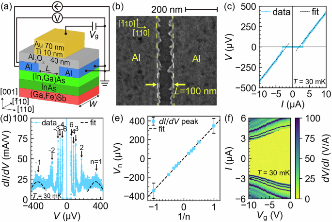
a Lateral Josephson junction device with a top gate electrode examined in this study. DC measurement setup is also shown. The junction length L and width W are 100 nm and 5 μm, respectively. b Scanning electron microscopy image of a junction device without a gate. The junction length is estimated to be ~100 nm at the longest part between the two Al electrodes. c Current dependence of the junction voltage (V – I characteristics) in a device without a gate at 30 mK. The dotted line represents interpolation from high-bias data using V = RN(I ± Iex). d Voltage dependence of dI/dV calculated from (c). The peak positions Vn correspond to multiple Andreev reflections, following Vn = 2Δ/ne. Peaks at n = ±1 are relatively broad and were fitted with Gaussian functions to estimate their positions. e Relation between the dI/dV peak voltages Vn and the inverse reflection order 1/n, extracted from (d). The error bars at n = ±1 show the standard deviation from Gaussian fitting shown in (d). f Dependence of the junction resistance dV/dI on the gate voltage Vg and bias current I. The current I was swept from negative to positive bias.
Figure 3c displays the V–I characteristics of an ungated junction at 30 mK. Unless otherwise stated, the V–I data were acquired by sweeping from zero to high bias currents in both plus and minus directions. The junction exhibits a zero-resistance state at low bias currents and nearly linear behaviour at higher currents. From these data, we extracted a critical current Ic = 3.00 μA, an excess current Iex = 1.91 μA, and a normal resistance RN = 52.5 Ω. Figure 3d shows the corresponding dI/dV spectrum, which exhibits several peaks resulting from multiple Andreev reflections (MARs)42. These peaks satisfy the relation Vₙ = 2Δ/ne, where Δ is the superconducting gap of Al and n is an integer constant, and are observable up to n = ±6. Although the n = ±5 peak is not clearly resolved and specific reasons are unclear, missing or weak individual higher-order peaks are not uncommon in MAR spectra43,44. Using the clearly resolved peak positions, a linear fit of Vₙ versus 1/n (Fig. 3e) yields a superconducting energy gap Δ = 171 μeV, which agrees well with that estimated from the critical temperature (Δ0 = 1.76kBTc = 196 μeV). The observation of MARs up to sixth order indicates sufficiently transparent Al/(In,Ga)As/InAs interfaces and an inelastic scattering length on the order of a few hundred nanometers, since high-order MAR processes require repeated Andreev reflections without inelastic relaxation. As shown in Fig. 3(f), even under applying a gate voltage Vg (<0 V), the MAR peaks persist, while the supercurrent decreases systematically with increasing |Vg| (negative Vg depletes electrons in the InAs channel). The positive Vg regime is discussed in Supplementary Material, where the critical current shows saturation under positive Vg. The leakage current remains below the order of 10 pA throughout the measured Vg range. These results demonstrate successful modulation of the critical current by electrostatic gating, which is important for practical device applications and provides further evidence for proximity-induced supercurrent through the semiconductor InAs layer.
The Josephson junction interface transparency can be quantitatively evaluated by parameters α = eIcRN/Δ = 0.92 and α′ = eIexRN/Δ = 0.59. The α value corresponds to 29%/44% of the ballistic/diffusive theoretical limits, and the α’ value corresponds to 22%/40% of the ballistic/diffusive theoretical limits, respectively45,46,47,48. While these data are not the highest among reported values, they exceed those of superconductor/semiconductor junctions prepared by sputtering and are comparable to those of epitaxially grown heterostructures49. These results confirm proximity-induced superconductivity with relatively high interface transparency in our Al/Fe-doped FMS heterostructures.
Next, we examined electrical transport under external magnetic fields in ungated (Fig. 4) and gated (Fig. 5) Josephson junction devices. Figure 4a, b show differential resistance as a function of perpendicular magnetic field B and bias current I when B is swept in opposite directions. Black arrows indicate the magnetic field sweeping directions, and Bini denotes the initialisation field applied to align the (Ga,Fe)Sb magnetisation before each measurement. The Fraunhofer patterns, where the superconducting regions are shown in yellow, exhibit unique and unconventional features that are distinctly different from the B-symmetric patterns in non-magnetic Josephson junctions50,51. In particular, the critical current Ic displays maxima at non-zero B, which have the same magnitude but opposite sign depending on the magnetic-field sweeping direction. Such hysteresis behaviour is consistent with a magnetic contribution to Josephson transport, possibly associated with ferromagnetism induced in the InAs channel by the adjacent (Ga,Fe)Sb layer. Moreover, there are several noteworthy features: unequal oscillation periods of the critical current between successive lobes; and non-monotonic decay of the Ic away from the central lobe, and numerous discontinuous points during magnetic-field sweeps, which we identify as flux jumps (the flux jumps, however, do not occur at exactly the same magnetic field across repeated measurements). These deviations from an ideal Fraunhofer pattern may arise from non-uniform magnetic-field and/or current distributions in the junction52,53,54. Such nonuniformity may also originate from the magnetisation reversal of magnetic domains in (Ga,Fe)Sb, which affects the magnetic-field distribution, and from accumulation of electrons at the two edges of the InAs channel, which will be discussed later. Trapped flux and vortex-related effects in the Al electrodes or junction region may contribute to the observed flux jumps and local distortions of the interference patterns. Likewise, variations in the effective junction length caused by edge roughness of the Al electrodes or inhomogeneous wet etching may produce spatial variations in the local Josephson coupling. However, these mechanisms alone are unlikely to account for the full set of observations. In particular, the Fraunhofer patterns exhibit a clear hysteresis between opposite magnetic-field sweep directions, and this behavior is reproducibly observed across multiple gated and ungated devices. The unconventional interference patterns therefore cannot be attributed solely to a field offset arising from trapped flux or vortices, or to static geometrical nonuniformity (see also Supplementary Material).
Fig. 4: Fraunhofer interference patterns, diode effect, and supercurrent distribution in an ungated Josephson junction.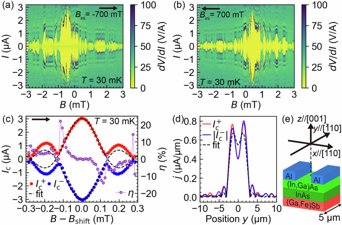
a, b Differential resistance of the junction without a gate as a function of magnetic field B and current bias I. Black arrows indicate the sweeping directions of B, and Bini denotes the initial field applied before sweeping. c Fine-field dependence of the critical current Ic and diode efficiency η. Bshift corresponds to the field at which the maximum critical current is observed in the measurement setup of (a). Black arrow indicates the magnetic field sweeping direction. No initial field was applied in this measurement. In all panels, the magnetic field is applied perpendicular to the junction plane. d Spatial distribution of the supercurrent density j flowing through the junction obtained by FFT analysis of the data shown in (c). The lateral axis position y (// [\(\bar{1}\)10]) shown in (e) corresponds to the in-plane direction perpendicular to the flowing current. e A schematic Josephson junction image without a gate with the definition of coordinate axes. The origin is set as the center position of the junction.
Fig. 5: Gate-voltage dependence of Fraunhofer interference patterns and critical currents.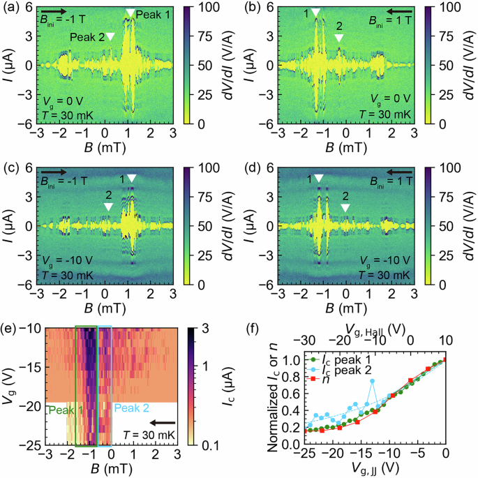
a–d Differential resistance of the gated junction as a function of the magnetic field B and current bias I. Black arrows indicate the sweeping directions of B, and Bini denotes the initial field applied before sweeping. a, b were measured at Vg = 0 V, while c, d were measured at Vg = −10 V. e Critical current Ic as a function of the magnetic field B and gate voltage Vg, used to identify the two regions with relatively large critical current, denoted as Peak 1 and Peak 2. Black arrow indicates the magnetic field sweeping direction. f Dependence of the normalised critical current Ic and carrier concentration n on the gate voltage Vg, normalised by their respective saturation values. Ic peak 1 is obtained at peak 1 from the field range −1.6 to −0.7 mT, and Ic peak 2 is obtained at peak 2 from −0.6 to 0 mT in (e). The sky-blue dashed line represents an exponential fit provided as a guide to the eye.
We conducted a fine-field scan around the maximum critical current (~−0.5 mT) in Fig. 4a, where Ic oscillations are observed without flux jumps, as shown in Fig. 4c. The horizontal axis represents the magnetic field relative to the center field Bshift (~−0.5 mT) defined as the point of maximal Ic. The oscillation period of 0.14 mT, which is determined with the fitting curve expressed by the conventional Fraunhofer equation Ic(B) = I0 sinc(πΓBS/Φ0), where Γ, S, Φ0 is a flux focusing factor, the junction size, and the flux quantum, is much smaller than the theoretical value of 1.13 mT estimated from the junction size. This indicates the effective flux focusing factor Γ of 8.2, likely including contributions from the Meissner effect of Al electrodes and stray fields from (Ga,Fe)Sb, magnetic proximity effect in the InAs channel, and inhomogeneity arising from possible magnetic domains or nonuniform current distributions53. Furthermore, the pattern is slightly skewed and the critical current exhibits pronounced nonreciprocity, with a diode efficiency η = (|Ic⁺| − |Ic−|)/(|Ic⁺| + |Ic−|) reaching 20% at the minimum of the Fraunhofer pattern (violet circles in Fig. 4c). Here, the superscripts ± denote opposite current directions. η is nearly antisymmetric with respect to the relative field B* = B − Bshift. The relations Ic⁺(+B*) ≠ Ic−(+B*) and Ic⁺(+B*) ≠ Ic⁺(−B*) manifest the broken time-reversal symmetry in the junction, which is also associated to proximity-induced magnetism in the superconducting InAs channel. The magnetic proximity effect may provide the time-reversal-symmetry breaking required for the superconducting diode effect7, while the asymmetric quantum-well potential and/or edge-channel transport can break spatial inversion symmetry. Therefore, the observed nonreciprocal critical current may arise from interaction of Rashba spin-orbit coupling and exchange field7,55, edge-channel superconducting transport discussed below, or a combination of both.
To gain a further insight into the junction characteristics, fast Fourier transformation (FFT) was performed on the Fraunhofer patterns where there is no flux jump, as shown in Fig. 4c. This narrow magnetic field range was selected because discontinuities caused by flux jumps or vortex motion can introduce artificial components into the Fourier-transformed current distribution. The FFT analysis provides a spatial mapping of the current distribution along the in-plane y-direction, which is perpendicular to the current flow, as illustrated in Fig. 4d, e. The details of the FFT procedure are described in Supplementary Material and in a reference56. The fitted current profile does not appear completely flat due to the limited number of lobes in the Fraunhofer pattern shown in Fig. 4c. The obtained current distribution indicates a tendency for the supercurrent to concentrate near the physical edges of the junction, in contrast to the more homogenous profile derived from the fitting curve expressed by a sinc function. Despite this edge-enhanced current profile, the SEM images show no discernible shortening of the junction length near the edges (Fig. S6). This indicates that the current enhancement at the edges cannot be attributed solely to geometrical variations at the edges of the Al electrodes.
As shown in Fig. 5a–d, Fraunhofer patterns at gate voltages of Vg = 0 V and −10 V under opposite sweeping directions of magnetic field consistently exhibit hysteresis behaviour depending on the sweeping direction; the overall shapes remain similar while the critical current decreases with applying gate voltage Vg. Figure 5e shows a colored map of the critical current Ic versus the perpendicular magnetic field, which has the same set up as those in Fig. 5b, d, when Vg is further swept from −10 V to −25 V. Two distinct regions with relatively large Ic are observed; peak 1 (from −1.6 to −0.7 mT) and peak 2 (from −0.6 to 0 mT). As shown in Fig. 5f, upon decreasing Vg the decay of Ic in peak 1 closely follows the decrease of the electron carrier density n in the InAs channel, which was obtained by Hall measurements at 5 K. This indicates that the change of Ic in peak 1 directly results from the depletion of Cooper pairs in the junction channel. On the other hand, the decay of Ic upon decreasing Vg in peak 2 is noticeably weaker than either that of peak 1 or the carrier density. This unusual behaviour suggests that superconducting transport in the junction involves multiple conduction channels, rather than a single uniform one, which is likely consistent with current density mapping obtained by FFT (Fig. 4d).
Furthermore, there are also pieces of evidence supporting edge channels in the Fraunhofer patterns upon closer inspection. First, the Fraunhofer patterns exhibit node-lifting, i.e., a nonzero critical current at the local minima of the pattern, as clearly observed in the first node (the nearest nodes from the maximum critical current) but not in the second nodes (the second nearest nodes from the maximum one) of the data in Fig. 4c. In conventional Fraunhofer interference, these minima should be zero. Previously, observations of node-lifting in the Fraunhofer patterns were attributed to the existence of edge channels, which are either topologically non-trivial57,58,59,60 or trivial61. Second, the maximum critical current in each lobe does not decay monotonically with the distance from the central lobe but instead alternates between large and small values—a phenomenon known as even–odd modulation. This can be clearly observed around 0.5 mT in Fig. 4a and −0.5 mT in Fig. 4b. The even−odd modulation occurs by the beating between h/2e (2e-transport) and h/e-periodicity (e-transport) of the Fraunhofer patterns62. While the h/2e periodicity is conventional, the h/e-periodicity is often associated with crossed Andreev reflections involving two edge channels61,63,64,65,66. In our junctions, however, this is opened to discussion considering that the estimated superconducting coherent length of Al thin film (~1.7 μm) is much shorter than the junction width (~5 μm). Nevertheless, these observations collectively point to the possible existence of superconducting edge channels, carrying both Cooper pairs and quasi-particles, in the InAs region.
Edge channels have indeed been reported at the two sides of InAs/(Ga,Fe)Sb heterostructures67. Under a perpendicular magnetic field, their normal conductance changes with opposite sign, producing large odd-parity magnetoresistance attributed to simultaneous breaking of time-reversal symmetry (via the magnetic proximity effect) and inversion symmetry at the edges. In the present junctions, the FFT analysis in Fig. 4d shows a slight asymmetry between the supercurrent densities at the two edges. Although this asymmetry is small and should be interpreted cautiously, it is consistent with the skewness of the measured Fraunhofer pattern and the nonreciprocal critical current shown in Figs. 4c and S5. The skewness of the Fraunhofer pattern may involve the asymmetric contributions from the edge channels, as suggested previously in twisted bilayer graphene Josephson junctions68. Further study is needed to fully understand the unconventional interference behaviour in these ferromagnetic junctions.
In conclusion, we have observed superconducting proximity effects in Josephson junctions fabricated from MBE-grown Al/InAs/FMS (Ga,Fe)Sb heterostructures. The junctions exhibit gate-tunable critical currents, a key feature for device applications exploiting semiconductor properties. Furthermore, they display Fraunhofer patterns with magnetic hysteresis, indicative of induced ferromagnetism in the superconducting InAs channel. Transport characteristics, including Fraunhofer interference, also provide possible evidence of edge-channel superconducting transport. Previously, a spin splitting energy of up to 18 meV has been observed in InAs when interfaced with (Ga,Fe)Sb containing 20% Fe and a Curie temperature of 300 K41. This spin-splitting energy is large enough to support a π-phase transition, as it significantly exceeds the Zeeman energy in semiconductors16,17,18,19 and is comparable to the exchange energy in diluted ferromagnets69,70,71. However, the (Ga,Fe)Sb used in this study has a Curie temperature of only 25 K and small remanent magnetisation (see Supplementary Material), resulting in a smaller spin-splitting energy that may be insufficient for reversing the phase of the superconducting wavefunction across the junction length, though it could help reduce spin-related scattering and enhance InAs mobility. The use of this 14.6%-Fe (Ga,Fe)Sb layer is a limitation of the present MBE growth process; although higher Fe concentrations would be preferable for enhancing the magnetic proximity effect, reproducible growth of higher-Fe-concentration (Ga,Fe)Sb layers compatible with subsequent Al/InAs heterostructure formation remains technically challenging. In the present devices, the gate dependence of the critical current is mainly attributed to carrier-density modulation in the InAs channel, and direct gate control of the exchange-induced spin splitting remains to be demonstrated. Therefore, Al–InAs/(Ga,Fe)Sb–Al heterostructures with improved magnetic properties, together with systematic studies using different junction lengths, will be required to realise π-phase transitions and to clarify the relative contributions of spin-singlet and spin-triplet components in the future work. These gate-controllable ferromagnetic Josephson junctions offer a promising platform for studying the coexistence of superconductivity and ferromagnetism and for developing new superconducting quantum devices.