
As Nvidia ships millions of Grace CPUs and Blackwell AI GPUs to data centers worldwide, the company is hard at work bringing up its next-generation AI and HPC platform, Vera Rubin, which is expected to set a new standard for performance and efficiency. Nvidia’s Vera Rubin comprises not one or two, but nine separate processors, each tailored for a particular workload, creating one of the most complex data center platforms ever.
While Nvidia will be disclosing more details about its Vera Rubin over the coming year before it officially launches in late 2025, let’s recap what we already know about the platform, as the company has revealed a fair few details.
At a glance
On the hardware side, Nvidia’s Vera Rubin platform is its next-generation rack-scale AI compute architecture built around a tightly integrated set of components. These include the following: an 88-core Vera CPU, Rubin GPU with 288 GB HBM4 memory, Rubin CPX GPU with 128 GB of GDDR7, NVLink 6.0 switch ASIC for scale-up rack-scale connectivity, BlueField-4 DPU with integrated SSD to store key-value cache, Spectrum-6 Photonics Ethernet and Quantum-CX9 1.6 Tb/s Photonics InfiniBand NICs, as well as Spectrum-X Photonics Ethernet and Quantum-CX9 Photonics InfiniBand switching silicon for scale-out connectivity.
You may like
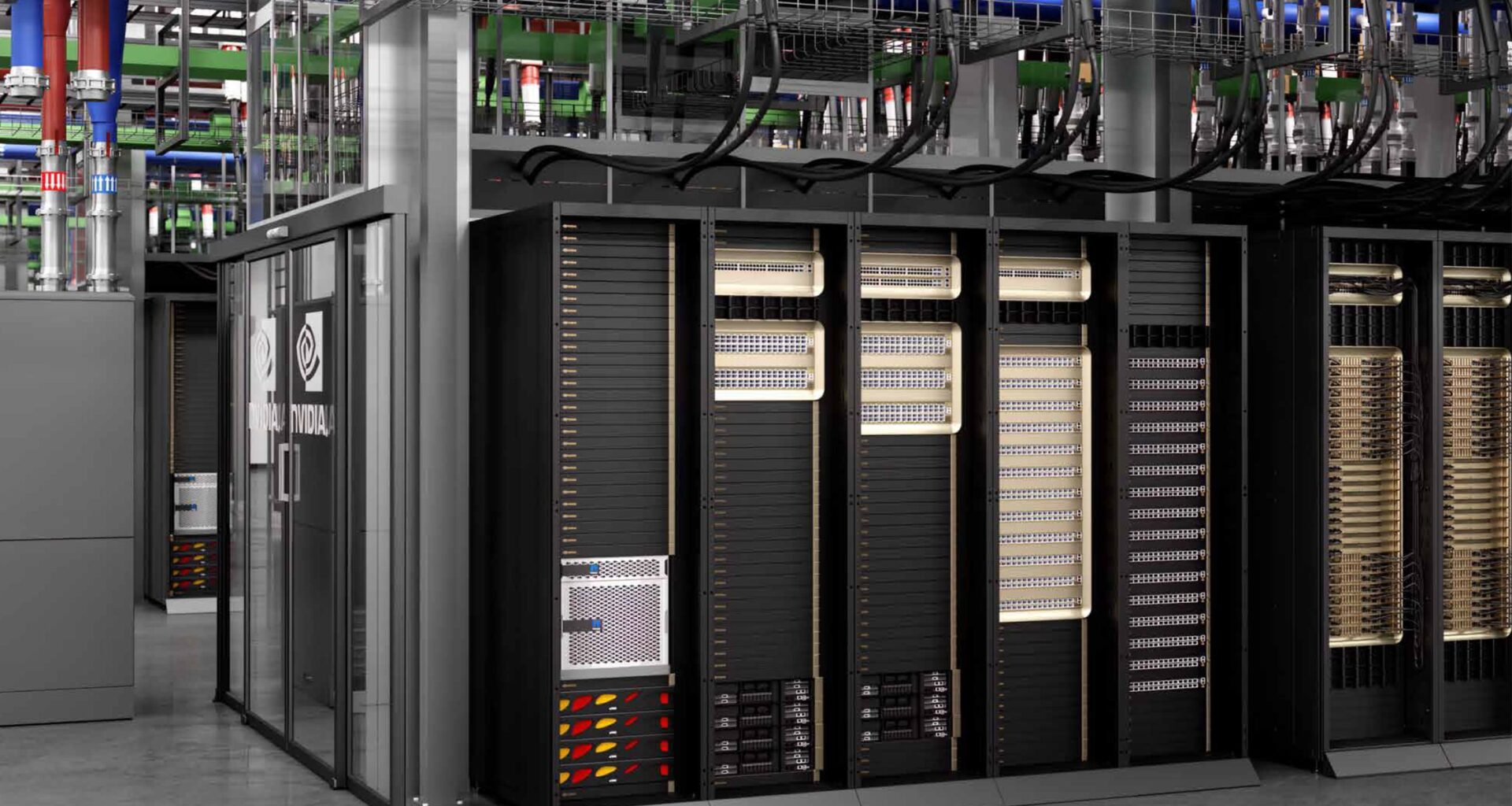
(Image credit: Nvidia/YouTube)
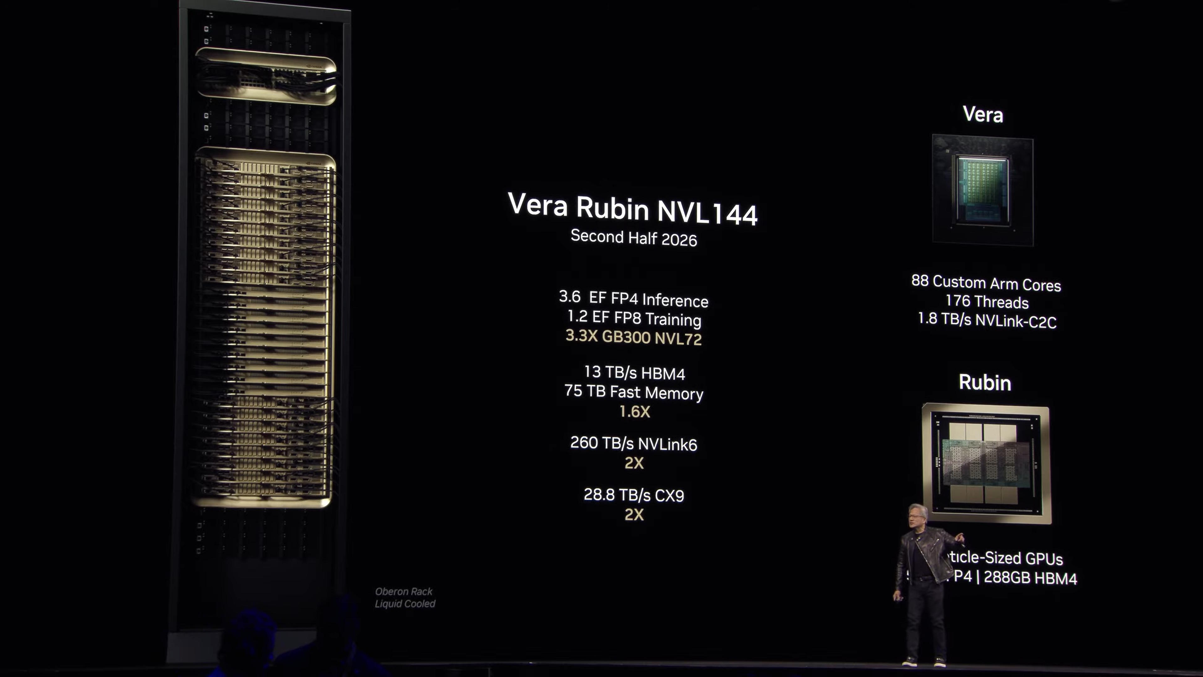
A full NVL144 rack integrates 144 Rubin GPUs (in 72 packages) with 20,736 TB of HBM4 memory and 36 Vera CPUs to deliver up to 3.6 NVFP4 ExaFLOPS for inference and up to 1.2 FP8 ExaFLOPS for training performance. In contrast, NVL144 CPX achieves almost 8 NVFP4 ExaFLOPS for inference using Rubin CPX accelerators, providing even more massive compute density.
On the software side, the Rubin generation is optimized for FP4/FP6 precision, million-token context inference, and multi-modal generative workloads. The CPX systems will come with Nvidia’s Dynamo inference orchestrator built atop CUDA 13, which is designed to intelligently manage and split inference workloads across different types of GPUs in a disaggregated system.
Additionally, Nvidia’s Smart Router and GPU Planner will dynamically balance prefill and decode workloads across Mixture-of-Experts (MoE) replicas to improve utilization and response time. Also, Nvidia’s Interconnect Extension Layer (NIXL) enables zero-copy data transfers between GPUs and NICs through InfiniBand GPUDirect Async (IBGDA) to reduce latency and CPU overhead. Meanwhile, NVMe key-value cache offload is said to achieve 50% – 60% hit rates, enabling multi-turn conversational context to persist efficiently. Finally, the new NCCL 2.24 library is expected to reduce small-message latency by 4x, enabling the scaling of trillion-parameter agentic AI models with much faster inter-GPU communication.
Truth to be told, these features are not specific to the Vera Rubin platform, but Rubin-class systems benefit the most from them, as the platform was designed explicitly to exploit them at scale. But what is so special about the Vera Rubin platform? Let’s dig a little bit deeper.
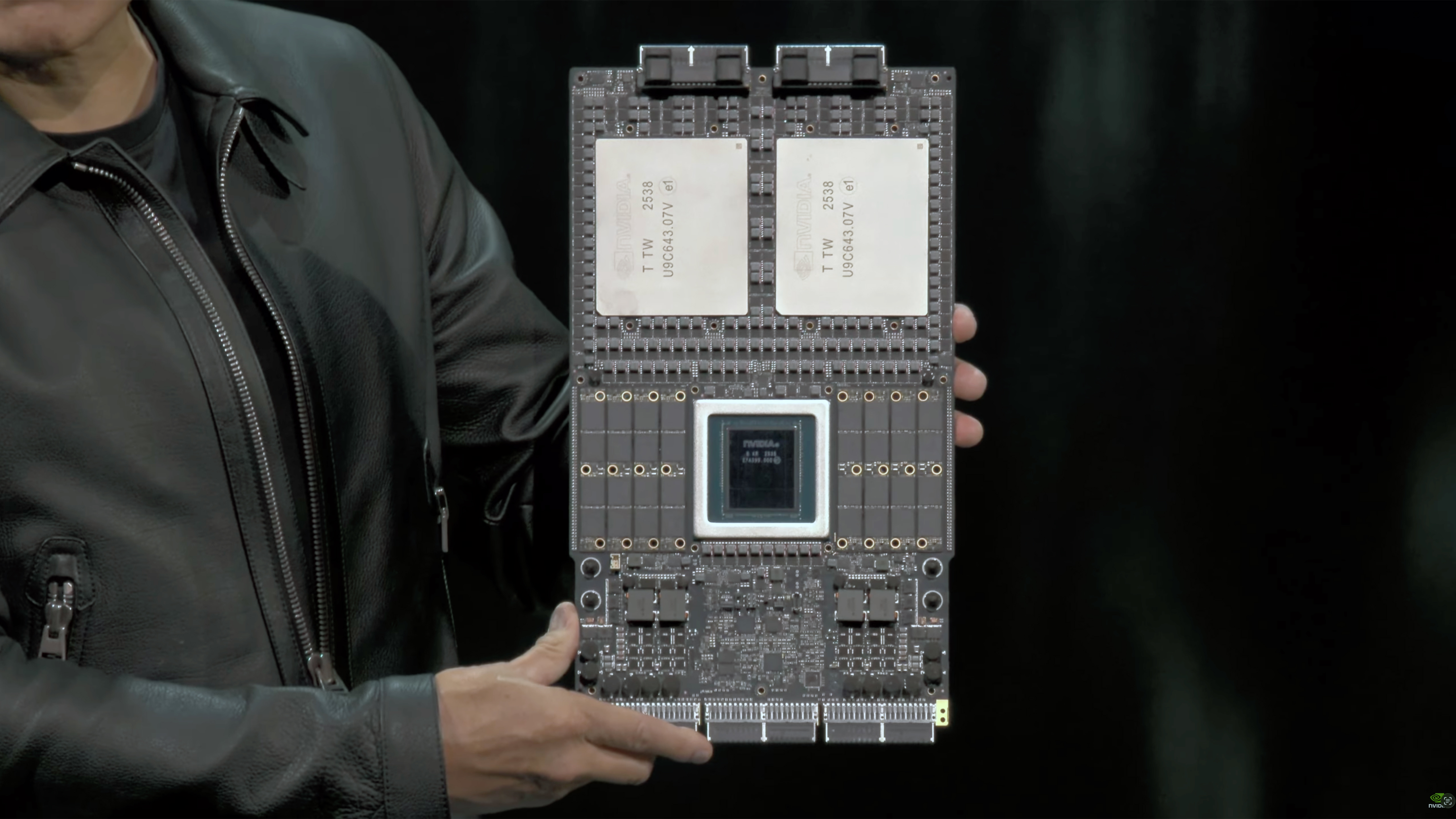
The Vera CPU
Nvidia’s Vera Rubin NVL144 and Rubin Ultra 576 platforms use Nvidia’s custom Vera processors specifically designed for data center-grade AI infrastructure and promising a two times performance increase compared to the predecessor, Grace.
(Image credit: Nvidia/YouTube)
The CPU packs 88 proprietary Armv9-class cores (a departure from Grace, which uses Arm Neoverse V2 cores) with 2-way simultaneous multithreading, enabling up to 176 threads to run simultaneously. These new Arm v9.2 cores, internally called Olympus, rely on a wide out-of-order pipeline and feature a wide set of optional extensions (SVE2, crypto, FP8/BF16, tagging, RNG, LS64, etc.). Nvidia’s documents indicate that SMT affects per-thread performance — e.g., most pipelines effectively halve per-thread throughput with two threads active, except for a few per-thread-dedicated ones, so developers should decide whether to use SMT for a given workload or keep one thread per core.
Nvidia continues to use its Scalable Coherency Fabric (SCF) within the CPU to tie cores and memory controllers together, but this time, the CPU’s memory bandwidth reaches 1.2 TB/s, 20% higher than Grace. As for system memory, Vera continues to use LPDDR5X, but now uses SOCAMM2 modules for extra density.
You may like
Vera uses NVLink-C2C as the coherent CPU to GPU link, the same technology as Grace-Blackwell, but with higher bandwidth. Grace offers 900 GB/s bidirectional bandwidth, but with the Vera Rubin platform, the bandwidth will double to around 1.8 TB/s per CPU.
The recently released images of the Vera processor show that the CPU does not appear to feature a monolithic design but a multi-chiplet design, as it has visible internal seams. One image shows that the Vera CPU has a distinct I/O chiplet located next to it. Also, the image shows green features emanating from the I/O pads of the CPU die; their purpose is unknown. Perhaps some of Vera’s I/O capabilities are enabled by external chiplets beneath the CPU, but this is merely speculation.
Publicly, there are still big gaps in information about Nvidia’s Vera CPU. There are no official clock speeds, per-core cache sizes, exact L2/L3 topology, or TDP. We also have limited information on NUMA/socket configurations outside the NVL144/NVL576 rack context.
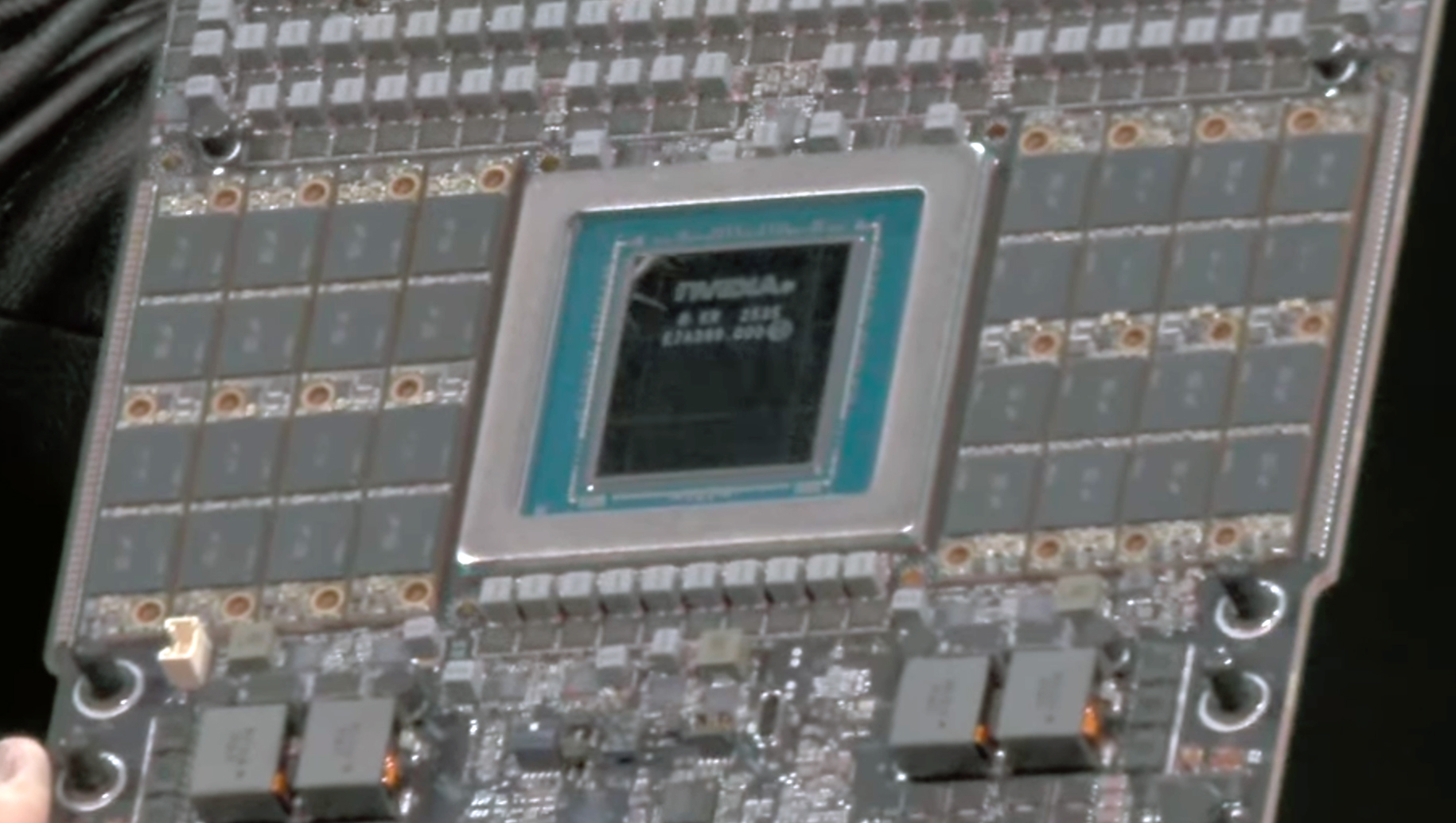
The Rubin GPU
The Rubin GPU is, without any doubt, the heart (or hearts, as there are two of them per board) of Nvidia’s Vera Rubin platform. The first Rubin GPU — let us call it R200 — features two near-reticle-sized compute tiles manufactured on a 3nm-class TSMC process technology, a pair of dedicated I/O dies, and 288 GB of 6.4 GT/s HBM4 memory arranged in eight stacks, offering roughly 13 TB/s of aggregate bandwidth. Note that starting from R200, Nvidia will count GPU dies, not GPU packages, as ‘GPUs’, thus although the NVL144 platform carries 72 GPU packages, Nvidia now sees them as 144 GPUs.
(Image credit: Nvidia)
Rubin GPUs are designed to push low-precision AI throughput for inference and agentic AI even further, but to boost training performance significantly too, compared to Blackwell Ultra, as Nvidia promises 50 FP4 PetaFLOPS and ~16 FP8 PetaFLOPS of performance per R200 GPU, which is 3.3 and 1.6 times higher than Blackwell Ultra, respectively. Nvidia has not yet outlined performance for higher-precision formats, but substantial generational gains are naturally anticipated.
Performance improvements will come with a clear tradeoff: power draw. Current guidance points to roughly 1.8 kW per GPU, which raises both infrastructure and cooling demands for large clusters. Yet, a 0.4 kW per GPU increase seems insignificant when 1.6X – 3.3X performance gains are present. Nvidia’s Vera Rubin NVL144 platform will continue to use the Oberon rack used for Blackwell/Blackwell Ultra NVL72, which appears ready to cool 1.8 kW GPUs with minor changes to its cooling system.
(Image credit: Nvidia)
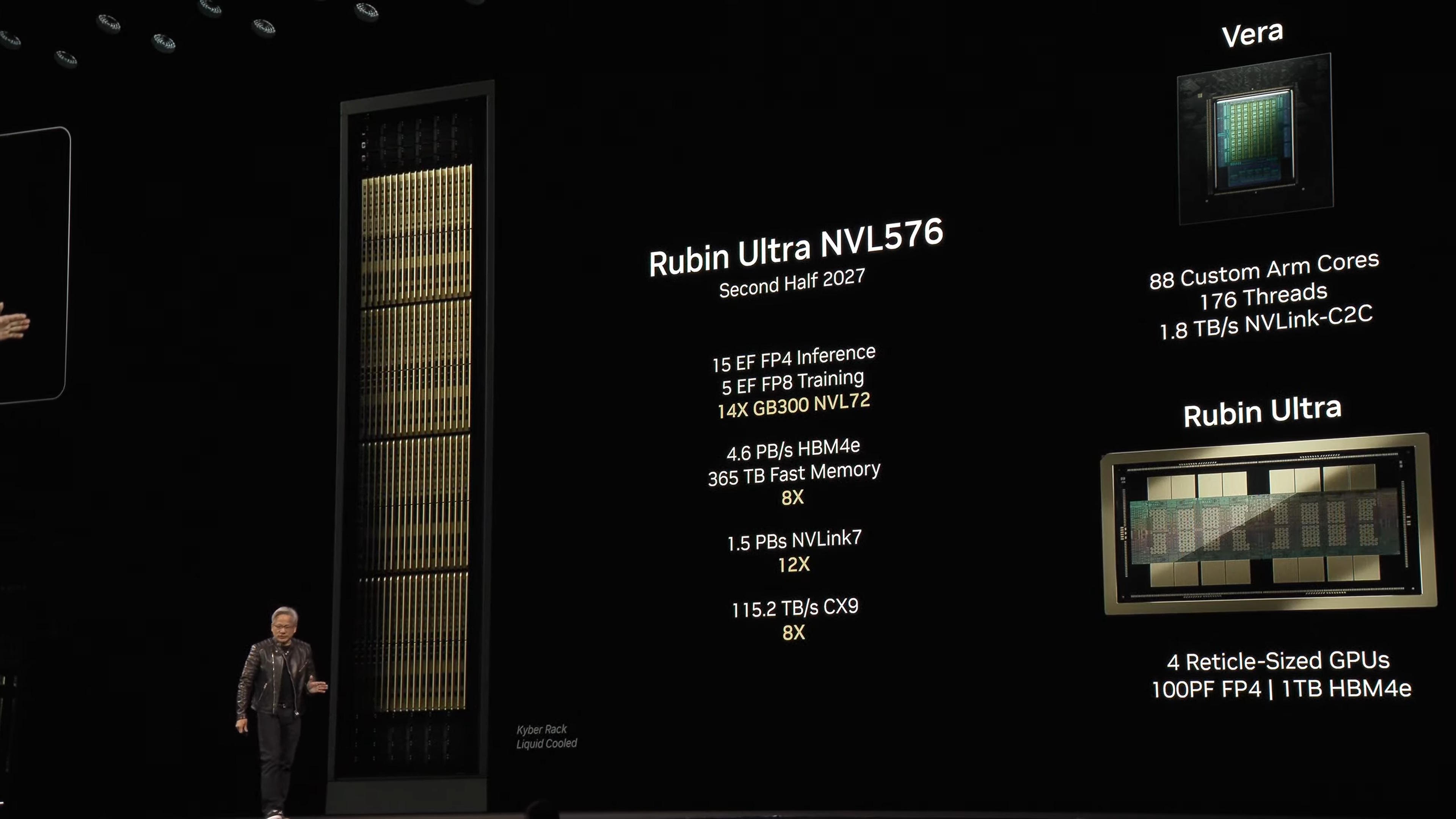
The follow-on refresh, known as the Rubin Ultra platform, is targeted for 2027 and aims to double performance by moving from two compute chiplets to four, which is expected to raise FP4 inference performance to around 100 PFLOPS per GPU package. The memory capacity of Rubin Ultra will also expand dramatically, reaching 1 TB of HBM4E, delivering approximately 32 TB/s of bandwidth. Such a configuration is projected to consume 3.6 kW, requiring an all-new cooling system for GPU packages and an all-new Kyber rack. In fact, Kyber will pack 576 GPUs in 144 GPU packages, thus significantly expanding Nvidia’s scale-up world size.
Both Rubin and Rubin Ultra are expected to rely on TSMC’s CoWoS-L advanced packaging technology. Rubin Ultra — which accommodates four near-reticle compute tiles, two I/O dies, and sixteen HBM4E stacks — likely uses a huge interposer, or combines multiple smaller interposers and stitches them together using bridges.
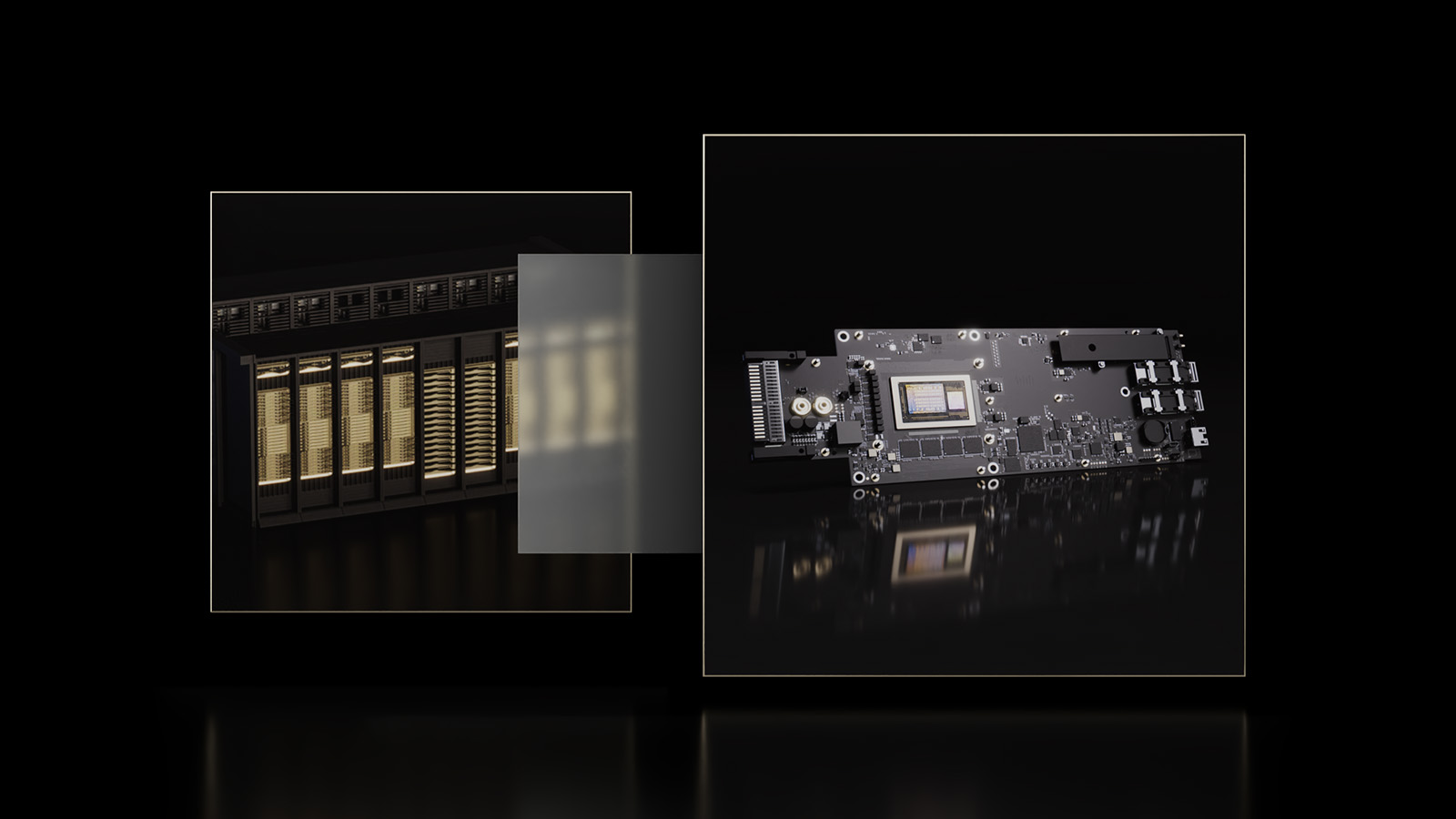
The Rubin CPX GPU
For the first time ever, Nvidia’s Vera Rubin NVL144 CPX will come equipped with an accelerator for accelerators: the Rubin CPX GPU, which will also be available for other platforms if their developers need it.
(Image credit: Nvidia)
Rubin CPX is a specialized inference accelerator built to handle the context-heavy front end of LLM workloads rather than the high-throughput generation phase. The GPU achieves roughly 30 NVFP4 PFLOPS of performance, which is lower than the flagship Rubin parts but well aligned with the workloads CPX is meant to accelerate.
Instead of the expensive and power hungry HBM4 stacks used on ‘full’ Rubin GPUs, CPX comes with 128 GB of GDDR7, which is cheaper, cooler, and does not require advanced packaging. This design gives CPX a large, cost-efficient memory pool for ingesting and encoding long sequences — consisting of hundreds of thousands to millions of tokens — and for managing multi-modal inputs such as video.
In the NVL144 CPX system layout, CPX runs alongside standard Rubin GPUs and the Vera CPU to process specific prefill/context workloads that Nvidia’s Dynamo software automatically offloads from the main GPUs. This division reduces both cost and power requirements for inference at scale, enabling datacenters to deploy large racks with optimal hardware for each stage of a model’s execution.
The BlueField-4 DPU
In addition to the specialized inference accelerator for prefill/context AI workloads, many NVL144 systems will include another accelerator, the BlueField-4 data processing unit. Instead of accelerating AI math, BlueField-4 accelerates everything around the GPUs — orchestration, networking, storage, and security, enabling systems to scale without putting an overwhelming load on CPUs.
(Image credit: Nvidia)
BlueField-4 integrates a 64-core Grace-based CPU, high-performance offload engines, and an 800 Gb/s network interface.
Functionally, BlueField-4 offloads the tasks that normally consume CPU cycles in massive clusters: packet processing, encryption/decryption, virtual switching, routing, telemetry, and storage operations such as NVMe-over-Fabrics or data reduction. By handling these operations in hardware, the DPU reduces latency, increases performance, and ensures that GPUs across many nodes stay fed with data. It also runs Nvidia’s DOCA framework, which provides microservices for security policies, multi-tenant isolation, monitoring, and virtualization.
Scale-up connectivity
Scale-up and scale-out connectivity are crucial components of Nvidia’s AI and HPC platforms, enabling clients to build hyperscale clusters based on Nvidia’s hardware with ease and predictable results.
Nvidia uses high-speed, low-latency NVLink fabric for linking CPUs (NVLink-C2C) and GPUs directly, while NVSwitch extends that fabric across all accelerators in a rack. With the Rubin generation in 2026, NVLink 6.0 is set to double its per-link throughput to about 3.6 TB/s total (1.8 TB/s each way), though it is unclear whether this comes from faster signalling or wider links. When paired with NVSwitch 6.0 inside systems like the NVL144, the full fabric can deliver roughly 28.8 TB/s of aggregate GPU-to-GPU bandwidth.
The 2027 Rubin Ultra refresh will move to NVLink 7.0 and NVSwitch 7.0, keeping the same bidirectional bandwidth per link but likely increasing the port count to around 144 per switch. This expanded switching capacity is what would let Nvidia interconnect the larger four-chiplet Rubin Ultra GPUs at full bandwidth across an entire rack and increase its scale-up world size to 144 GPU packages.
Scale-out connectivity
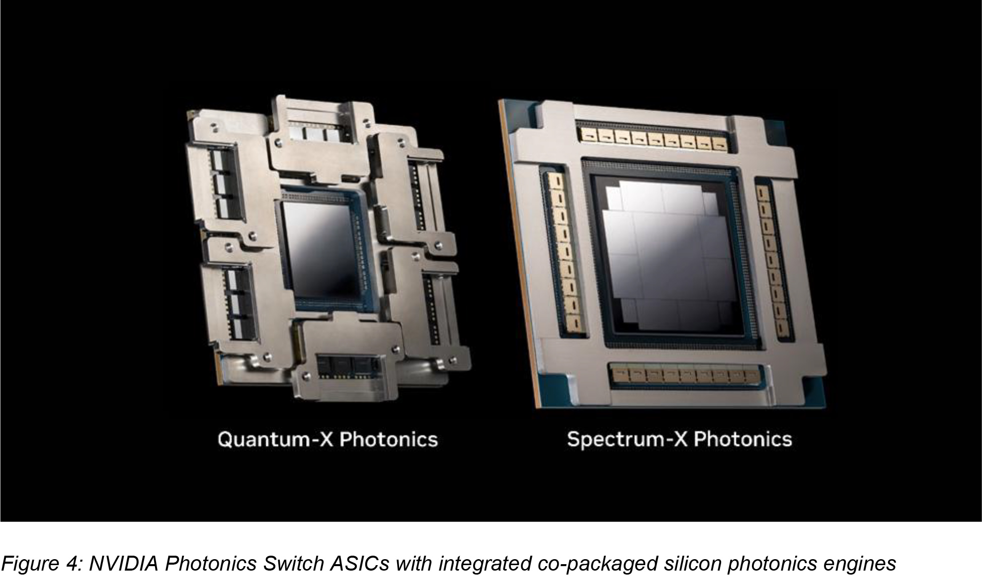
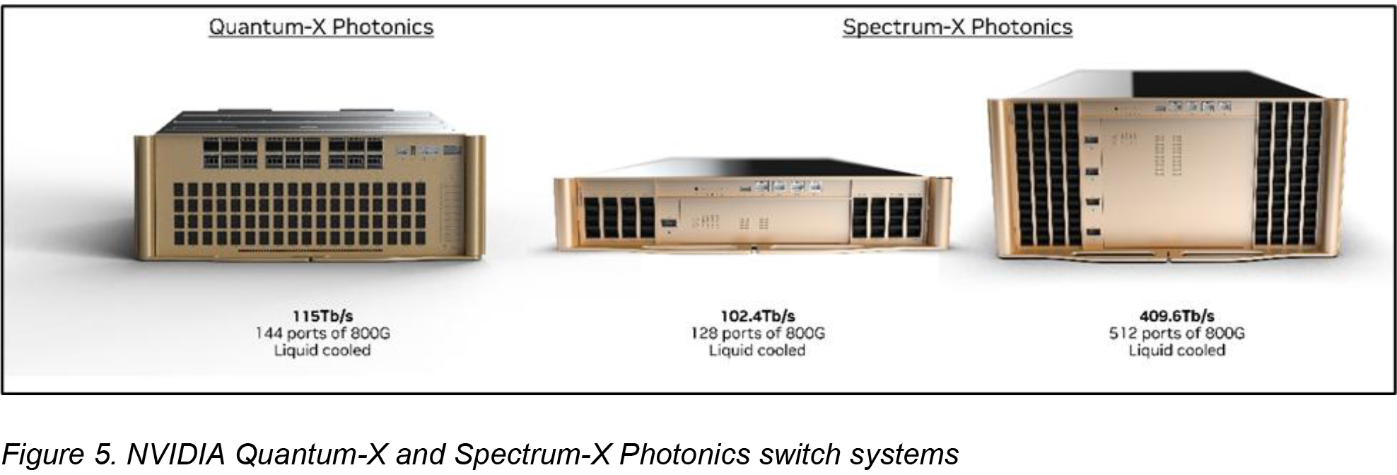
For scale-out connectivity, Nvidia will introduce co-packaged optics (CPO) optical interconnection platforms — consisting of both network cards and switching silicon — for Ethernet (Spectrum-X) and InfiniBand (Quantum-X) technologies on its Rubin generation platform and onwards.
(Image credit: Nvidia)
At a high level, both Nvidia’s Spectrum-X Photonics Ethernet and Quantum-X Photonics InfiniBand platforms are based on TSMC’s 1st Generation COUPE platform that integrates a 65nm electronic integrated circuit (EIC) with a photonic integrated circuit (PIC), delivering up to 1.6 Tb/s per port.
Nvidia’s photonics rollout begins with Quantum-X InfiniBand switches that are set to arrive in early 2026 and aim to deliver 115 Tb/s of fabric bandwidth through 144 lanes at 800 Gb/s, or eventually 576 lanes at 200 Gb/s. These platforms include an integrated processing ASIC capable of 14.4 TFLOPS to accelerate in-network operations via Nvidia’s SHARP v4 protocol to reduce collective-operation latency. All Quantum-X units are designed with liquid cooling to manage their thermal load.
On the Ethernet side, Spectrum-X will ship switches in multiple port-density options: 128×800 Gb/s or 512×200 Gb/s, both offering around 100 Tb/s of aggregate throughput. A larger model increases capacity to 512×800 Gb/s or 2,048×200 Gb/s, reaching 400 Tb/s in total.
(Image credit: Nvidia)
At the recent GTC event in October, Nvidia introduced the ConnectX-9 Spectrum-X SuperNIC, a next-generation 1.6 Tb/s network interface built specifically for large-scale AI clusters. The unit packs and extremely high-bandwidth SerDes, a PCIe 6.0 48-lane switch, and fully programmable RDMA capabilities to give GPUs a direct, low-latency path into Spectrum-X Ethernet and Quantum-X InfiniBand fabrics. The card is designed to enable zero-copy GPU-to-network data movement (through GPUDirect Async and NIXL) and significantly reduce CPU involvement in multi-node inference and training workloads.
Architecturally, ConnectX-9 is the endpoint that ties NVLink-connected racks, such as NVL144 or NVL576, to photonics-enabled scale-out networks, enabling Rubin- and Rubin Ultra–class systems to sustain the massive bandwidth required for multi-rack AI clusters. It also includes a secure on-board platform for isolation and telemetry, and provides the foundation for the high-density configurations of up to hundreds of NICs per cluster rack, which will likely become common with NVL144 and NVL576 systems.
We will update this page as we learn more about Nvidia’s upcoming Rubin architecture.

Follow Tom’s Hardware on Google News, or add us as a preferred source, to get our latest news, analysis, & reviews in your feeds.