
Structures of R- and H-stacked WSe2/WS2/WSe2 heterotrilayers
We fabricated dual-gate WSe2/WS2/WSe2 heterotrilayer devices, which allow independent control of doping levels and vertical electric field (Fig. 1a, see Methods). The structure of heterotrilayers investigated is shown in Fig. 1b inset. We highlight the layer alignments with arrows: parallel indicating R stacking and opposite indicating H stacking. Device 1 (Fig. 1b optical image) displays the top WSe2 layer aligned with the middle WS2 layer at an angle close to 1° (R stacking), while the bottom WSe2 layer is rotated 180° with a slightly different alignment angle (H stacking). This device also includes a bilayer region for direct comparison.
Fig. 1: Structural characterization of trilayer heterostructure Device 1.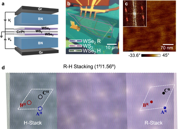
a Schematic of a dual-gated WSe2/WS2/WSe2 heterotrilayer device, in which pre-evaporated and AFM-cleaned Cr/Pt is used as contacts to the TMD layers. b Optical image of Device D1 highlights the alignment of top WSe2 and bottom WSe2 layers relative to the middle WS2 layer, with the top WSe2, middle WS2, and bottom WSe2 outlined in purple, pink, and green, respectively. Inset: Schematic illustrating layer alignments with arrows indicating R stacking (parallel) and H stacking (opposite). c PFM image of Device D1’s trilayer region, revealing two distinct moiré superlattices with lattice constants of approximately 7.4 nm ( ~ 0.9°) and 6.7 nm ( ~ 1.5°), marked with red dashed circles in the inset Fourier transform image. d An exemplary trilayer with a top moiré with a 1° rotation (R-stack) and a bottom moiré with a 1.56° rotation (H-stack), with high-symmetry sites A, B, C denoted by blue, red, and black circles; hollow symbols mark H-stack sites (AH, BH, CH) and filled symbols mark R-stack sites (AR, BR, CR). The R- and H-stack moiré superlattices form a concatenated moiré pattern across the trilayer.
Moiré superlattices can be clearly identified in the Piezoresponse Force Microscopy (PFM) image of Device 1’s trilayer region (Fig. 1c). Fourier transform data (Fig. 1c inset) reveal two distinct moiré superlattices with lattice constants approximately 7.4 nm ( ~ 0.9°) and 6.7 nm ( ~ 1.5°). Besides, a larger superlattice background could be identified in the PFM image emerging from the interference of these two sets. This small, deliberate twist-angle offset of roughly 0.5° keeps each bilayer well aligned and prevents severe global disorder and frustration, while preserving the beating patterns (see Supplementary Information Fig. S1).
Unlike previous experimental studies focusing on symmetric alignment in the top and bottom heterostructures37,38,39, the intricate interplay of high-symmetry stacking configurations in the R-H misaligned heterotrilayers unveils the elusive atomic registry textures. As depicted in Fig. 1d, an exemplary trilayer exhibits a top moiré with a 1° rotation (R-stack) and a bottom moiré with a 1.56° rotation (H-stack). Following the convention from Tong et al36, these R- and H-stack moiré superlattices form a concatenated moiré pattern across the trilayer, delineated by nine distinct high-symmetry locales (Supplementary Information Fig. S2), each exhibiting different band hybridization between the top and bottom layers. At locales such as AR/AH (similar for BR/BH, CR/CH in Fig. S2), conservation of spin-valley degrees of freedom is anticipated to suppress tunneling and hybridization. By contrast, high-symmetry locales such as AR/CH may allow stronger hybridization, depending on the local atomic alignment.
In reported heterobilayers, the spatial distributions of band-edge electrons differ between R-stack and H-stack heterostructures40. In R-stack heterobilayers, electrons are localized predominantly at the high-symmetry location CR, whereas in H-stack heterobilayers, they are mostly found at location AH. Combining R and H stackings in heterotrilayers likely generates multiple orbital configurations for electrons centered in the middle layer, where both A and C serve as trapping sites. The physics inherent in R-H style heterotrilayers promises a tapestry of intriguing phenomena.
Multi-orbital nature of the bichromatic moiré superlattice
The multi-orbital nature of the bichromatic moiré superlattice promotes the tunability of valley and spin degrees of freedom in TMD heterotrilayers. Experimentally, this manifests as multiple photoluminescence (PL) peaks in the heterotrilayer structure. The PL spectrum (Fig. 2a) reveals a dominant low-energy emission at ~1.39 eV and a secondary, weaker peak at ~1.46 eV. The energy separation of ~70 meV between the two peaks significantly exceeds the expected exciton double occupancy energy ( ~ 30 meV) at a single moiré site26, indicating a multi-orbital origin. Power-dependent PL measurements on Device 3 (Fig. S3) show that both peaks persist even at the low excitation power, confirming their intrinsic origin from the heterotrilayer moiré potential rather than from power-induced filling effects. The normalized power dependence of the lower energy peak (Fig. S4) shows significant saturation behavior. The above evidence confirms that the emissive excitonic species from heterotrilayer regions are intrinsic to the bichromatic moiré potential.
Fig. 2: Electric field dependence of interlayer PL peaks.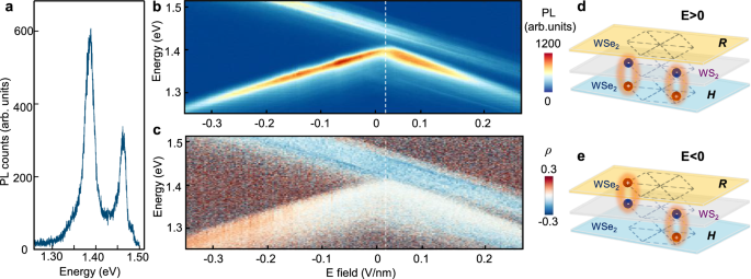
a PL spectrum of the trilayer heterostructure, displaying a dominant low-energy peak at 1.39 eV (low-energy peak) and a secondary peak at 1.46 eV (high-energy peak). b Interlayer PL as a function of electric field without external doping possesses different slopes of the Stark shift across positive and negative electric field regimes. c The corresponding PL degree of circular polarization ρ = \(\frac{{{{\rm{\sigma }}}}^{+}/{{{\rm{\sigma }}}}^{+}-{{{\rm{\sigma }}}}^{+}/{{{\rm{\sigma }}}}^{-}}{{{{\rm{\sigma }}}}^{+}/{{{\rm{\sigma }}}}^{+}+{{{\rm{\sigma }}}}^{+}/{{{\rm{\sigma }}}}^{-}}\) in the same conditions as in b. The high-energy peak remains cross-polarized regardless of field direction, whereas the low-energy peak flips from cross- to co-polarized when the electric field is reversed from positive to negative. d-e, Schematics of preferred sites of interlayer exciton emission with positive electric field (d) and negative electric field (e). The yellow, grey, and blue layers denote top WSe2 (R stacking), middle WS2, and bottom WSe2 (H stacking). Blue and red spheres indicate electrons and holes, respectively. The low-energy peak originates from sites where holes can redistribute freely between the top and bottom WSe2 layers (the left side in d, e), whereas the high-energy peak comes from sites where holes remain localized in the bottom WSe2 layer (the right side in d, e). In this study, positive electric field points from the top WSe2 to the bottom WSe2, and negative electric field points from the bottom WSe2 to top WSe2 layer.
To probe the origins of the dual PL peaks, we conducted out-of-plane electric field measurements while keeping the doping fixed. Upon applying an electric field without external doping, both PL peaks exhibit clear linear Stark shifts (Fig. 2b). These linear Stark shifts correspond to the emissions originating from the interlayer excitons possessing significant out-of-plane dipoles.
The emission energy of the high-energy peak decreases monotonically with the applied electric field. This peak is attributed to the interlayer exciton, with its dipole moment oriented downward. The interlayer exciton arises from the binding of holes in the bottom WSe2 layer and electrons in the middle WS2 layer. Polarization analysis, shown in Fig. 2c, further supports the identification of this high-energy exciton. The peak exhibits cross-polarization (ρ < 0), indicating that the emission originates from an H-stack WSe2-WS2 heterobilayer40. This agrees with mid-bottom bilayer configuration.
In contrast, the low-energy peak shows opposite slopes when the sign of the electric field is reversed. These opposing slopes, observed in Fig. 2b, c, correspond to dipole moments that flip direction. This behavior confirms that the lower-energy exciton exhibits a bipolar emission characteristic. The dipole moment of this interlayer exciton (IX) flips dynamically with the applied electric field, with hole polarization occurring either in the top R-stacked layer or the bottom H-stacked layer (as shown in Fig. 2d, e).
At a small electric field near E = 0.02 V/nm, the low-energy interlayer excitons emitted from the top R-stacked and bottom H-stacked layers exhibit identical energies. In this range, the local slope of the low-energy peak is flat. This flat slope matches the quadrupolar excitons observed in symmetric heterotrilayers37,38,39. Despite differences in periodicity and stacking order between the top and bottom moiré superlattices, the identical energies and flat local slope are a signature of a shared ground state in the R-H aligned heterotrilayers. Additional data from another Device D2 is present in Supplementary Information Fig. S5.
The unique features of the PL peaks are attributed to the multi-orbital characteristics of the heterotrilayers. As illustrated in Fig. S2, the heterotrilayers feature multiple high-symmetry sites arising from the beating of the top and bottom moiré superlattices. Excitation of intralayer excitons in WSe2 leads to rapid carrier relaxation to the band edges, forming interlayer excitons. At minimally hybridized sites, the excitons retain the same dipole moment. As a result, excitons emitted from these sites exhibit a single slope, as shown in Fig. 2b. By contrast, at strongly hybridized sites the lowest-energy state is shared by both the top and bottom layers. In this case, an applied electric field polarizes holes toward the bottom WSe2 layer (for E > 0) or the top WSe2 layer (for E < 0). Consequently, the bound excitons at these sites develop a positive or negative dipole moment depending on the direction of the electric field.
Although the excitons share the same lowest-energy at specific high-symmetry locations, the distinct stacking orders of the top and bottom bilayers enforce opposing selection rules. The low-energy PL peak for E < 0, characterized by a positive slope, exhibits a positive degree of polarization (Fig. 2c), which is consistent with the R-stack configuration in the upper heterobilayer of our device. In contrast, interlayer excitons in the lower heterobilayer, with negative slopes, display a negative degree of polarization, aligning with the H-stack configuration. This layer-polarized emission introduces an additional degree of freedom for manipulating circular polarization while maintaining fixed emission energies.
Quadrupolar moiré trions
Under hole-doping conditions, our experiments reveal the presence of quadrupolar excitonic emission in the moiré trilayers, as shown in Fig. 3a, b. Additional data across varying doping conditions from Device D1 are presented in Fig. S6. Furthermore, data from Device D2, tested under similar conditions, is included in Fig. S7. The formation of quadrupolar excitonic species occurs immediately upon introducing excess holes into the heterostructure. To confirm the formation of interlayer trions, we deliberately dope the heterotrilayer at fixed hole concentrations while sweeping the electric field. Figures 3a, b show two hole-doping conditions at n = –2.25 × 1012 cm2 and n = –3.75 × 1012 cm–2. The low-energy peak exhibits minimal shifts in emission energy under low-field conditions (additional hole doping scenarios are shown in Fig. S6). The flat slope confirms an almost negligible out-of-plane dipole moment. In contrast, the high-energy peak shifts negatively with the electric field, consistent with the behavior observed in Fig. 2b under intrinsic doping conditions. This shift is attributed to the fixed out-of-plane dipole moment of the exciton, whose position in the moiré superlattice results in a small hybridization probability, as illustrated in Fig. 2d, e.
Fig. 3: PL peaks’ positions shift as a function of the electric field under fixed doping conditions.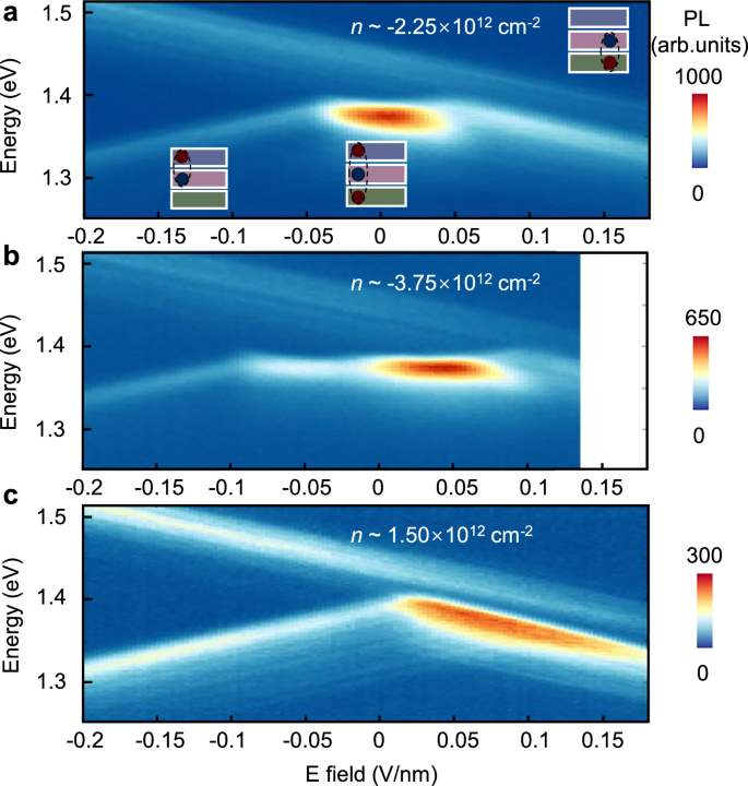
a n = –2.25 × 1012 cm–2, b, n = –3.75 × 1012 cm–2, c, n = 1.5 × 1012 cm–2. Under hole doping (a and b), the peak energy of the low-energy peak remains nearly constant over a finite electric-field window, indicating the stabilization of a quadrupolar trion, whereas no such signature appears under electron doping (c). The inset of a schematically present, from right to left, the carrier configurations that yield the low-energy peak: holes localized in the bottom WSe2 layer under positive electric field and pair with an electron in the middle WS₂ layer to form an interlayer exciton; holes shared between the top and bottom WSe2 layers create a quadrupolar trion; and holes once again confined to the top WSe2 layer bind to the middle-layer electron under negative electric field, forming another interlayer exciton. The blue and red circles represent electrons and holes located in the WS2 and WSe2 layers, respectively. The blue, pink and green rectangles denote the top WSe2, middle WS2 and bottom WSe2 layers.
Under electron doping conditions, the flat slope of the low-energy peak is absent (Fig. 3c). The observed slopes are directly ascribed to the dipoles associated with the top and bottom interlayer excitons.
We attribute the excitonic species with nearly zero out-of-plane dipole moments to the formation of quadrupolar moiré trions under hole-doped conditions. This interpretation is consistent with a scenario in which two holes are symmetrically distributed across the WSe2 layers (Fig. 3a middle inset), regardless of whether the structure is R-stack or H-stack aligned. Strong Coulomb interactions drive the emergence of this unique three-particle complex, where two holes and one electron are strongly localized at the shared high-symmetry moiré sites. The resulting interlayer quadrupolar trion exhibits a nearly vanishing out-of-plane dipole moment, and its energy remains stable under varying electric fields, clearly distinguishing it from previously reported interlayer trions in heterobilayers8,9,41. Importantly, unlike the bosonic quadrupolar excitons observed in symmetric trilayers37,38,39 that exist primarily under charge-neutral conditions, quadrupolar moiré trions appear only under doping. Furthermore, they require a substantially larger electric field to polarize into dipole configurations. This enhanced robustness indicates that the formation of interlayer quadrupolar moiré trions is energetically favored in bichromatic heterotrilayers.
When the electric field becomes sufficiently strong, holes in the bottom (top) WSe2 layer are polarized to the top (bottom) WSe2 layer to minimize the total energy, resulting in a well-defined out-of-plane dipole moment. Specifically, for hole density below –2 × 1012 cm–2 ( ~ ν = –1 for one moiré), a modest electric field of approximately ±0.025 V/nm is sufficient to transform the quadrupolar trion into a dipolar exciton (Fig. S6d, e). In this regime, polarized holes can redistribute across different moiré sites within the same WSe2 layer, effectively lowering the total energy. However, at higher hole fillings ν ≥ –1, polarizing all holes into the same layer forces them to share moiré sites, incurring strong on-site Coulomb repulsion. Consequently, a larger field exceeding ±0.05 V/nm is needed to overcome this repulsion and achieve full dipolar polarization. These experimental findings demonstrate that the electric field can effectively tune the ground states of holes by manipulating their layer-specific degrees of freedom.
Electric-field modulation of the moiré potential landscape
We now deliberately tune the electric field to control the distribution of doped holes. As shown in Fig. 4a, b, at E = 0 V/nm, the shared ground state results in an even hole distribution across the top and bottom layers, with both WSe2 layers experiencing the same moiré potential landscape. When the carrier density reaches 3.6 × 1012 cm–2, we observe a change in PL intensity (Fig. 4a) and enhanced polarization (Fig. 4b). This behavior aligns with the formation of an interlayer Mott insulating state, as reported by Lian et al39. However, in our study, this phenomenon occurs in an asymmetric heterotrilayer, characterized by distinct R-stack and H-stack layers, contrasting with the symmetric R-R stack with identical lattice constants in the top and bottom layers as described in previous work39. It’s worth noting that, the interlayer Mott insulating state observed here differs from the behavior seen in regions with only bilayer R-stack heterostructure. In the R-stack heterobilayer, as shown in Fig. S8, holes are strictly confined to the top WSe2 layer, and intensity variations occur at both fractional and integer filling factors.
Fig. 4: PL intensity and polarization as a function of doping with a fixed electric field.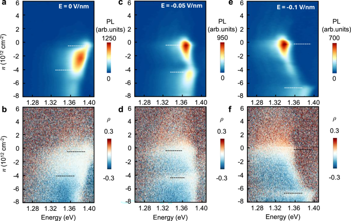
a–b, PL intensity (a) and polarization (b) versus density with E = 0 V/nm. c–d, PL intensity (c) and polarization (d) versus density with E = –0.05 V/nm. e–f, PL intensity (e) and polarization (f) versus density with E = –0.1 V/nm. The PL intensity and polarization changes are used to identify the integral filling and insulating states, ν = 0 and ν = –1 can be clearly discerned and marked by dashed lines in both the PL (white dashed lines) and corresponding polarization (black dashed lines) 2D maps. The corresponding density in ν = –1 under the electric field of 0 V/nm, –0.05 V/nm and –0.1 V/nm is 3.6 × 1012 cm–2, 4 × 1012 cm–2 and 6.45 × 1012 cm–2, respectively. Line cuts of the raw data illustrating the polarization changes under specific conditions are provided in the Supplementary Information as Fig. S11.
When a fixed negative electric field (–0.05 V/nm) is applied, the doped holes would predominantly occupy the top WSe2 layer. At a hole carrier density of 4 × 1012 cm–2, strong intensity modulation (Fig. 4c), and a significant decrease in polarization (Fig. 4d) are observed, as labelled by the dashed lines. The observed intensity and polarization modulations are consistent with previously reported signatures of correlated states in TMD heterobilayers19,25,26,27,40,42. It is worth noting that the emergence of integer-filling correlated states provides compelling evidence that the PL peaks originate from excitons localized at bichromatic moiré sites. The abrupt changes in PL intensity and polarization with doping, as shown in Fig. 4 and Figs. S8–10, are indicative of strong interactions between interlayer moiré excitons and correlated electronic states, consistent with prior observations in moiré systems19,25,26,27,40,42.
By further tuning the electric field, the moiré potential profile is significantly altered, as shown in Fig. 4e, f. For a fixed electric field of –0.1 V/nm, we observe a surprising increase in the doping density required to reach the insulating state, rising to approximately 6.45 × 1012 cm–2. Furthermore, a distinct blueshift is observed at this point, indicative of the onset of on-site Coulomb repulsion. The substantial increase in carrier density needed to form the insulating state strongly suggests a shift in the density of ground-state sites.
Similar behavior is observed in Device D2 (Fig. S9). The electric field required to reshape the entire moiré landscape is slightly different, owing to the variation in twist angles between the R-stack and H-stack layers. As shown in Fig. S10, the moiré superlattice of the H-stack heterobilayer is approximately 7.6 nm, which is slightly larger than the value measured in Device D1 from the PFM data. However, qualitatively, the behavior with the applied electric field remains consistent with what we observed in Device D1.
To gain insight into the experimental observations, we have calculated the moiré potentials for valence band holes in heterotrilayer bichromatic superlattices, following the methodology outlined by Tong et al36. Detailed calculations are provided in the Supplementary Information. The concatenated moiré pattern is visualized by tracing several high-symmetry stacking sites, as shown in Supplementary Fig. S1, which includes both R-stack and H-stack high-symmetry regions. The calculated moiré potentials under various electric field conditions are presented in Fig. 5. The bright regions represent the local potential minima for holes (i.e., the valence band maximum). These regions will be first populated when the system is hole-doped.
Fig. 5: Calculated electric-field modulation of moiré superlattice potential landscape in real space.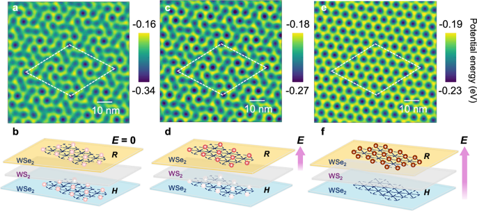
Moiré superlattice potential in the heterotrilayer without electric field (a), at electric field of –0.05 V/nm (c), and at electric field of –0.1 V/nm (e). The bright yellow locales are potential minima for holes. b,d,f, Schematics showing the preferred layer localization of holes under the corresponding electric field conditions. As the out-of-plane electric field is swept from 0 to –0.05 V/nm and then to –0.1 V/nm, the number of hole-potential minima increase significantly, and the hole distribution shifts toward the top WSe2 layer, accompanied by a transition of the Mott insulating state from interlayer to intralayer. The yellow, grey, and blue slabs represent the top WSe2 (R stack), middle WS2, and bottom WSe2 (H stack) layers, respectively. Colored spheres indicate holes localized in two WSe2 layers, with darker shading corresponding to higher hole density.
Considering the geometry of the trilayer moiré superlattice (Fig. 1d), we find that the heterotrilayer exhibits distinct moiré potential profiles compared to heterobilayers, with the added advantage of dynamic tunability via an applied electric field (Fig. 5). The simulations in Fig. 5 are performed under similar conditions to the measurements in Fig. 4. In Fig. 4a, b, the applied electric field is zero. At this condition, the hole density corresponding to the first integer filling insulating state, identified as an interlayer Mott insulator, is approximately 3.6 × 1012 cm–2, which is notably higher than the density required to reach ν = 1 in the R-type heterobilayer with a moiré wavelength of 7.4 nm (n ~ 2.1 × 1012 cm–2). In the absence of an electric field, the simulated moiré potential (Fig. 5a) shows bright regions slightly larger than the R-type stacking domains (Fig. S12), with multiple high-symmetry sites available for hole occupancy. As shown in Fig. 5b, the holes are distributed across both the upper and lower WSe2 layers, forming a degenerate interlayer configuration. Laterally, the hole is confined to a common moiré potential minimum shared between layers, resulting in one hole occupying a shared ground state at the same high-symmetry moiré site in the hybridized trilayer. This correlated state is referred to as an interlayer Mott insulator39. In this regime, the holes can redistribute between the top and bottom WSe2 layers within the same vertical moiré cells.
As the electric field increases (E-field pointing from the bottom gate to the top gate) to –0.05 V/nm, the hole density required for the Mott insulating state increases to 4.0 × 1012 cm–2 (Fig. 4c, d). The corresponding simulation shows the area of the bright regions expands slightly, indicating an enhanced capacity for hole occupancy (Fig. 5c). In this regime, holes preferentially occupy sites in the upper layer, with fewer holes residing in the lower layer (Fig. 5d). At an even higher electric field of –0.1 V/nm, the hole density at ν = –1 further increase to 6.45 × 1012 cm–2 (Fig. 4e, f). The simulated potential landscape evolves into a honeycomb-like pattern (Fig. 5e), effectively doubling the number of sites available for hole localization, consistent with our experimental observations. In this regime, the electric field fully polarizes the doped holes to localize in the upper layer (Fig. 5f), where the correlated states are now governed by intralayer hole interactions with modified moiré periodicity and enhanced Coulomb repulsion. The strong on-site repulsion energy results in a significant blueshift in the excitonic emission. Overall, these results demonstrate that the applied electric field in a bichromatic moiré superlattice enables a tunable transition from interlayer- to intralayer-dominated Mott insulating states.
We realize that the role of strain relaxation in real devices would affect the moiré superlattice landscape. In complex trilayer structures, the R-stack and H-stack regions relax strain differently40. However, our calculations provide a qualitative physical framework for understanding the role of the electric field in modulating moiré potentials and hole distribution within the superlattices. These findings strongly support the realization of electrically tunable bichromatic moiré potentials.