
Semiconductor lasers are a class of devices in which the light is generated via stimulated emission in a semiconductor gain media. They are employed in various applications due to the small device size, monochromaticity, high light density, and coherence.
The vertical-cavity surface-emitting laser (VCSEL) is a type of semiconductor laser, in which a gain medium is encapsulated between two distributed Bragg reflectors (DBRs), and light is emitted from the device surface. VCSELs are electrically pumped; because of it the DBRs need to be doped to act as contact layers. The need for contacts on the same surface, from which light is emitted, limits the emission area of the final device, and leads to technological difficulties in the growth.
To overcome this limitation, the vertical-external-cavity surface-emitting-laser (VECSEL) gain chip, in which the upper DBR is substituted by an external coupler, was developed. The external cavity geometry is suitable for optical pumping, and grants access to the laser cavity for the insertion of intracavity elements such as saturable absorber for mode locking1, nonlinear crystals for frequency doubling2 or multiple VECSEL chips increasing output power while keeping high beam quality3,4,5. Another more key feature of VECSEL is the output power scalability. VECSELs have been demonstrated with output power from 0.5 W6 up to 106 W7 without sacrificing beam quality. This power scalability comes from the possibility of increasing the pump power on the VECSEL chip by increasing the surface that is pumped.
Lasers generating 976 nm light find applications both as a pumping source for erbium doped fiber, and for the generation of 488 nm light via second harmonic generation (SHG)8. In the case of 976 nm wavelength VECSEL the maximum output power recorded was 20 mW9. The limiting factor was the pumping area; lasing was not observed for areas with diameter greater than 50\(\upmu\)m. The demonstrated pumping area is consistent with other published results10,11.
Different combinations of materials can be used to fabricate the DBR and the multiple quantum wells (MQW). For VECSEL with 976 nm emission, AlAs and GaAs for the DBR growth and InGaAs/GaAs for the MQWs are most often used.
To maximize the output power density of the device it is necessary to suppress In segregation, and avoid the formation of dislocations in the QW structure. In the active area, it is necessary to grow quantum wells with very defined In content and quantum well width to be able to select the correct emission wavelength. It was demonstrated that high substrate temperature during molecular beam epitaxy (MBE) growth has a strong effect on In segregation to the surface of the QW layer, this in turn has been shown to affect shape and energy of the photoluminescence (PL) spectrum12,13,14.
The main focus of the investigation of InGaAs MQWs in the last five years is on the improvement of quantum confinement using AlGaAs barrier15,16, micro-characterization of optical properties of nanoscale structures such as nanospades17 and studies on the improvement of quality structures in low temperature growth conditions and high strain structures18,19,20.
Indium segregation can be suppressed via kinetic limitation, either by limiting the As overpressure or by growing the sample at lower substrate temperatures21. However, both approaches lead to a lower crystalline quality and weaker PL intensity12. The lower growth rate (400 nm/h) has also been shown to lead to sharper interfaces between the QW and barrier layers, enhancing the optical efficiency of the structure22,23.
In Fitzgerald et al.24 it was demonstrated that lattice dislocations act as non-radiative recombination centers; they lead to a drop in PL emission intensity and result in the presence of a net of reduced PL intensity. The presence of these non-radiative recombination centers affects the emitters in two main ways: it reduces the overall efficiency of the gain chip, decreasing the output power and leads to the generation of localized heat in the device25.
To avoid lattice dislocations, strain compensation is usually used. In particular InGaAs/GaAs QWs can be compensated by GaAsP layers placed at the nodes of the optical field of the VECSEL26,27. Another possible solution is to use the so called diluted nitrides; this approach consists in alloying low nitrogen content, typically less than 2 %, in the InGaAs QWs, reducing the In content needed to obtain an emission at the same wavelength, with the net effect of reducing the lattice mismatch28,29,30,31. The main drawback of this method is that the incorporation of nitrogen generally leads to the formation of point defects. Therefore, the use of designs that do not require to employ strain balancing strategies is highly desirable.
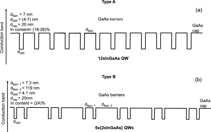
This work is focused on optimization of the MBE growth process for application of InGaAs QWs separated by GaAs barriers in VECSEL active area emitting at 976 nm. Both QW thickness and In content were varied to achieve the target emission wavelength. Investigations were performed for large areas using room temperature photoluminescence (RTPL) and micro-photoluminescence (\(\upmu\)-PL), in order to determine the influence of the composition of the QW and the barrier design on the optical quality of the heterostructures.