
 An example of the HM and OLEDs at work together – credit, University of St. Andrews
Until now, holograms have been created using lasers, but now researchers have used a new ensemble of components that could unleash this technology on the market.
With their ubiquity in science fiction, and carrying the potential to transform smart devices, communication, gaming, and entertainment, holograms would be a major technological advancement, if we could find an easier way of projecting them.
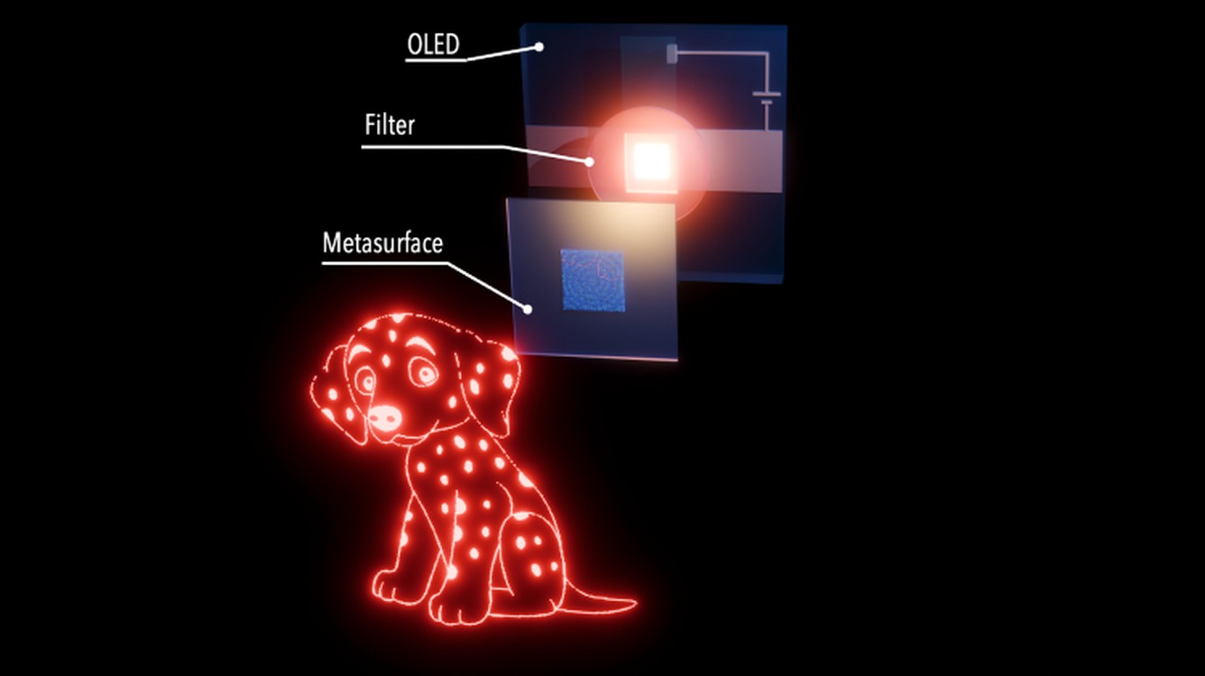
A team at the University of St. Andrews have found that ‘Holographic Metasurfaces’ (HMs) and Organic Light Emitting Diodes (OLEDs) give a simpler and more compact approach that is potentially cheaper and easier to apply, overcoming the main barriers to hologram technology being used more widely.
Organic light-emitting diodes are thin film devices widely used to make the colored pixels in mobile phone displays and some TVs. As a flat and surface-emitting light source, OLEDs are also used in emerging applications such as optical wireless communications, biophotonics, and sensing, where the ability to integrate with other technologies makes them good candidates to realize miniaturized light-based platforms.
A holographic metasurface is a thin, flat array of tiny structures called meta-atoms—the size of roughly a thousand of the width of a strand of hair. They are designed to manipulate light’s properties, and can make holograms and their uses span diverse fields, such as data storage, anti-counterfeiting, optical displays, high numerical aperture lenses, optical microscopy, and sensing.
This, however, is the first time both have been used together to produce the basic building block of a holographic display.
Researchers found that when each meta-atom is carefully shaped to control the properties of the beam of light that goes through it, it behaves as a pixel of the HM. When light goes through the HM, at each pixel, the properties of the light are slightly modified.
Thanks to these modifications, it is possible to create a pre-designed image on the other side, exploiting the principle of light interference, whereby light waves create complicated patterns when they interact with each other.
HI-TECH INNOVATION: Outer Space Is the Place for Manufacturing Cancer Drugs, Says Startup Using Crystal Technology
This technical explanation from the university perhaps doesn’t capture the gravity of the development. Professor Graham Turnbull, from the School of Physics and Astronomy at St. Andrews, offered his version in a release from the university press.
“OLED displays normally need thousands of pixels to create a simple picture. This new approach allows a complete image to be projected from a single OLED pixel!”
MORE TECHNOLOGIES LIKE THIS: This Bracelet from Meta Translates Hand Movements into Computer Actions
Until now, researchers could only make very simple shapes with OLEDs, which limited their usability in some applications. However, this breakthrough provides a path toward a miniaturized and highly integrated metasurface display.
“Holographic metasurfaces are one of the most versatile material platforms to control light,” said Andrea Di Falco, professor in nano-photonics at the School of Physics and Astronomy. “This breakthrough will enable a step change in the architecture of holographic displays for emerging applications, for example, in virtual and augmented reality.”
SHARE This With Your Friends Who Love A Bite Of Hi-Tech News…