
First principle calculations of electron and phonon properties of SbxSey films
The calculated dielectric permittivities ε∞ (electronic contribution) and εion (ionic contribution) of Sb2Se3 crystal (Table 2) are in acceptable agreement with the experimental ones presented in Ref21. To our knowledge, Ref21. provides a detailed experimental study of the reflection spectra and corresponding dielectric functions of Sb2Se3 single crystals in the far-infrared range, as well as a theoretical study of the phonon modes for the crystal at the orthorhombic space group of symmetry Pnma (no. 62).
In the present study, instead, the experimental reflection spectra of Sb2Se3 polycrystalline films deposited on soda-lime-glass substrates are measured in the far-infrared range. The stoichiometry and crystal structure of these polycrystalline films may differ from the corresponding features in the above-mentioned Sb2Se3 single crystals. Furthermore, first-principles calculations based on density functional theory of the Sb₂Se₃ single crystal were performed, taking into account the van der Waals interaction, and the corresponding dielectric function was obtained. The imaginary part of this dielectric function is used for comparison with the experimental reflection spectra of the studied Sb₂Se₃ films. The present study aims to provide more information on the electron and phonon properties of both stoichiometric and non-stoichiometric Sb2Se3 crystals, which may be utilized for the practical applications of Sb2Se3 films in solar cell technology.
According to the analysis of the accuracy of the experimental dielectric function curves ε(ν) performed in Ref21., the accuracy of determining the electronic dielectric permittivity ε∞ was estimated to be about 20%, while the corresponding error for the ionic dielectric permittivity, Δεion/εion, can be larger. The relative differences between the averaged theoretical (row 5 of Table 2) and experimental (row 6 of Table 2) dielectric permittivities are presented in row 7 of Table 2. The obtained relative differences 2×|εt – εe|/(εt + εe), appear acceptable when considering that the theoretical and experimental accuracies of determining the dielectric permittivity are both approximately 20%. The characteristic feature of Sb2Se3 crystal is the large anisotropy of the calculated dielectric permittivity tensor ε: the contributions to the averaged dielectric permittivity from the y- and z-directions of the crystal are much larger than that from the x- one (Table 2). The spontaneous electric polarization in Sb2Se3 crystal and SbxSey deposited films is not expected because the space group of symmetry Pnma is nonpolar. The absence of polar symmetry in SbxSey films may be partly caused by the relatively small difference of antimony and selenium electronegativities, χ(Se) – χ(Sb) = 0.5 (Pauling scale), which corresponds to the relatively small ionic character (IC)40 of Sb Se bonding, IC = %. Small ionic character of Sb Se bonds may cause small Sb Se dipole moments in SbxSey films, which can decrease the probability of polarized parts arising in these films during their deposition on a substrate.
Table 2 Calculated cartesian components of the macroscopic static dielectric permittivities, ε∞ (electronic contribution) and εion (ionic contribution), of Sb2Se3 crystal at the space group of symmetry Pnma (no. 62) calculated for GGA-PE, GGA-PS, and GGA-MK + vdW exchange-and-correlation functionals.
It is known13 that the interatomic bonding in Sb2Se3 crystal is strongly anisotropic because the covalently bonded (Sb4Se6)n ribbon-like structure elements are realized along one of the crystallographic directions ([001]) and weaker forces take place in the two other orthogonal directions. Very high anisotropy of the dielectric properties in Sb2Se3 is observed for the ionic part of the dielectric permittivity, εion_x < < εion_y, εion_x < < εion_z (Table 2). Similar but not so high anisotropy of the dielectric properties in Sb2Se3 takes place for the electronic part of the dielectric permittivity, ε∞x < ε∞y, ε∞x < ε∞z (Table 2). The observed anisotropy of the dielectric permittivity tensor corresponds to the layer-like crystal structure of Sb2Se3, for which the corresponding quasi-layers are perpendicular to the [100] direction (a-direction) (Fig. 5). Thus, the comparatively weak van-der-Waals interaction is realized between the quasi-layers with boundaries indicated in the b-cut view of Sb2Se3 crystal structure by the thick horizontal lines (Fig. 5). The relatively weak van-der-Waals interaction in [100] direction of the crystal is a reason for the much smaller ionic and smaller electronic parts of dielectric permittivity in this direction in comparison to [010] and [001] ones (Table 2). No layer-like crystal structure is found in the [010] direction (b-direction).
Fig. 5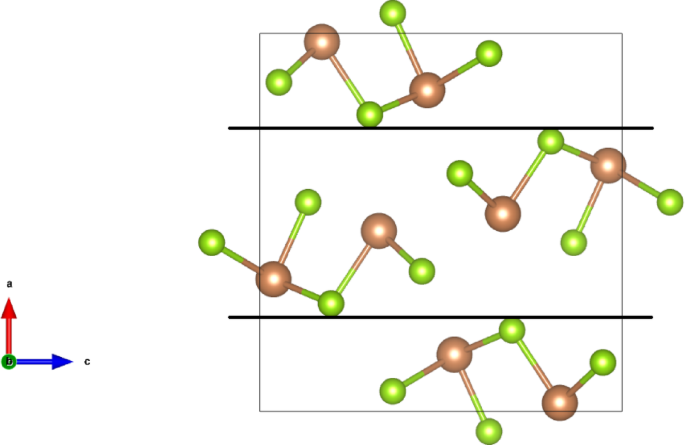
The b-cut view of Sb2Se3 crystal structure at Pnma (no. 62) space group of symmetry. Thick horizontal lines indicate planes of boundaries between structural layers perpendicular to the a-axis of the crystal’s unit cell.
Dispersion of the phonon energy bands of Sb2Se3 crystal is observed in the frequency range of 0–220 cm−1, where the acoustic modes are realized in the range of 0–50 cm−1 and the optical modes are observed in the range of 50–220 cm−1 (Fig. 6a, b). The phonon dispersions of Sb2Se3 calculated for PBE and PBEsol exchange-and-correlation functional are close to one another (Fig. 6a, b). Negative frequencies were observed in the dispersion dependence ν(Q), calculated without taking into account the vdW interaction and this happened in the Q-segments Γ X and Z – U, where the Q[100] component was changing. This result is caused by the relatively weak interatomic interaction in the [100] direction of the crystal (Fig. 5). Another manifestation of the relatively weak interatomic interaction in the [100] direction of the crystal is the flat dispersion dependences ν(Q) at the segments S – Y, Z – U, and R – T, where the changes of the type, [0QyQz] ↔ [\(\frac{1}{2}\)QyQz], of the phonon Q-points in the Brillouin zone take place.
Fig. 6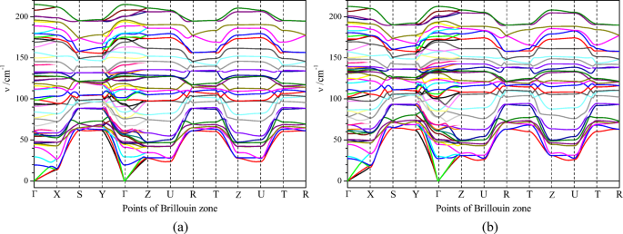
Dispersions of phonon energy bands of Sb2Se3 calculated with using van-der-Waals interaction of DFT-D3 method of Grimme41,42 at (a) PBE and (b) PBEsol exchange-and-correlation functionals. The correspondence of the Brillouin zone symbols and Q-points is following: Γ[000], X[\(\frac{1}{2}\)00], S[\(\frac{1}{2}\)\(\frac{1}{2}\)0], Y[0\(\frac{1}{2}\)0], Z[00\(\frac{1}{2}\)], U[\(\frac{1}{2}\)0\(\frac{1}{2}\)], R[\(\frac{1}{2}\)\(\frac{1}{2}\)\(\frac{1}{2}\)], T[0\(\frac{1}{2}\)\(\frac{1}{2}\)].
Fig. 7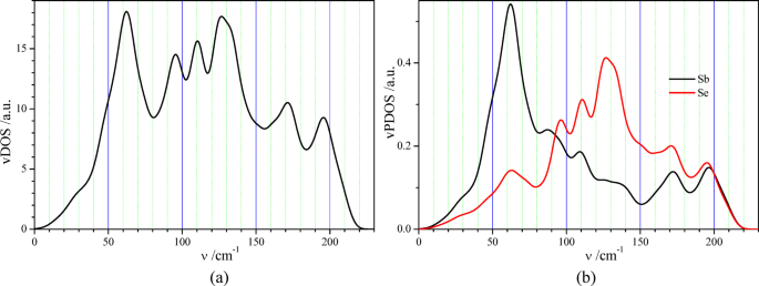
(a) Vibration density of states vDOS and (b) vibration partial density of states vPDOS of antimony and selenium atoms in Sb2Se3 crystal calculated at PBE exchange-and-correlation functional.
The calculated vibration total and partial densities of states (vDOS and vPDOS) of Sb2Se3 crystal (Fig. 7) are characterized by numerous maxima, which correspond to the numerous groups of phonon energy bands (Fig. 6). Clear hybridization of the antimony and selenium vibration states is observed, which is manifested by the equality of the frequency positions of vPDOS(Sb) and vPDOS(Se) maxima (Fig. 7b). The characteristic feature of these vPDOS is a dominance of the antimony density of states in the frequency range 0–90 cm−1 and a dominance of the selenium density of states in the range 90–190 cm−1 (Fig. 7b). The latter feature is expected because of the larger atomic mass of antimony atom (M(Sb) = 121.76) in comparison to the mass of selenium one (M(Sb) = 78.971).
The results of our DFT-based calculations of lattice dynamics of Sb2Se3 crystal have shown that the corresponding infrared phonon excitations take place in the frequency range of 50–220 cm−1. According to these results, the spectral range above 220 cm−1 should be the range of crystal transparency, if some other mechanisms of radiation absorption are absent. However, from the SEM and EDX results of the deposited films, we also expect the metallic phase of the redundant antimony, which can be the source of free electrons. These free electrons may cause the inverse proportional dependence of the reflection coefficient R on the frequency ν43.
Reflection spectra in the far-infrared spectral range SbxSey films
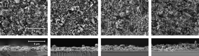
Analysis of SbxSey reflection spectra R(ν) shows the presence of an interference-like structure in the frequency range of ν > 1200 cm−1 for several samples (Fig. 8a). The distances between neighboring interference extrema for samples no. 3, 4, and 7 correspond to film thicknesses of about 1 μm, which are close to the values determined by the other method (Table 1). The absence of a clear interference-like structure for other films in Fig. 8a can be caused by the relatively strong radiation scattering on their rough surfaces. This suggestion is in agreement with the observed quasi-monotonous decrease of the reflection coefficient R with the increase of the frequency ν, caused by the surface roughness, which is expected for the mean surface roughness of about 0.5 μm (see the cross-sections of films in Fig. 1).
Fig. 8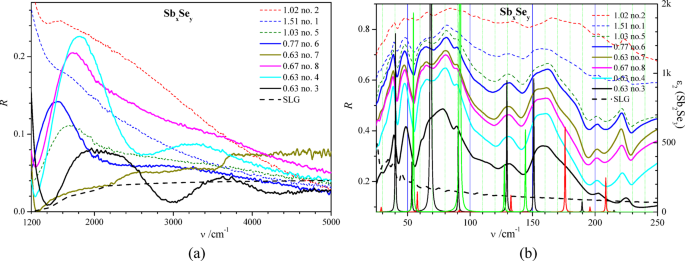
(a) Reflection spectra R(ν) of eight SbxSey films on soda-lime glass substrates (SLG) and SLG measured at room temperature. The legend values correspond to the index of compound relation x/y determined from EDX measurements and sample number (Fig. 2b, d). The values of R correspond to the absolute reflection coefficients. The experimental calibration of the R scale was performed using the gold mirror and its known optical constants. (b) Reflection spectra R(ν) of eight SbxSey films on soda-lime glass substrates (SLG) and SLG measured at room temperature and theoretical spectra of imaginary part of dielectric permittivity ε2(ν) (narrow black, red and green peaks). Here, for ε2(ν) spectra, black, red and green colors correspond to the light polarizations along x-, y-, and z-axis of Sb2Se3 crystal at the space group of symmetry Pnma (no. 62). The legend values correspond to the index of compound relation x/y determined from EDX measurements and sample number (Fig. 2b, d). The values of R correspond to the absolute reflection coefficients. The experimental calibration of the R scale was performed using the gold mirror and its known optical constants.
The reflection spectra R(ν) in the range ν < 230 cm−1 are presented in Fig. 8b for SbxSey films studied. The largest reflection coefficients are observed for the samples 1, 2 and 5 (Fig. 8b). This is caused by the increased amount of metal phase of antimony in the deposited films and, consequently, by the increased reflection coefficients due to Drude-like behavior in the far-infrared range43. The mean value/level of the reflection coefficient of SbxSey films in the range of 25 230 cm−1 (Fig. 8b) is proportional to the concentration of residual antimony atoms (Fig. 2b), being in the metal-like state, compared to their bonded states in the Sb2Se3 polycrystals.
The reflection spectra of SbxSey films in the far-IR range are similar because of the almost identical positions of R(ν) peaks (Fig. 8b). The highest similarity is observed for the spectra of samples 4–8, which may confirm the formation of the same crystalline phase Sb2Se3 in these samples. These positions are in good quantitative agreement with the positions of maxima of the imaginary part of the dielectric function ε2(ν) obtained from our first-principle calculations of Sb2Se3 crystal within the framework of DFT (Fig. 8b). The structure of the reflection spectra R(ν) measured for SbxSey films (Fig. 8b) is rather similar to that obtained experimentally for Sb2Se3 single crystals21. The latter was also observed in a similar spectral range, 25–210 cm−1, and was characterized by a similar number of reflection maxima. One of the clear differences between the experimental reflection spectra of the Sb2Se3 films studied (Fig. 8b) and the reflection spectrum of an Sb2Se3 single crystal is the reflection maximum in Sb2Se3 films in the range 221–225 cm−1 (Fig. 8b), which is absent in this frequency range in Sb2Se3 single crystal21. This should be caused by the vibration mode associated with the special states of selenium ions in Sb2Se3 films, which are absent in the corresponding single crystal. This should be associated with the selenium ions, first of all, because the vibration states of selenium ions are characterized by a larger vPDOS compared to the vPDOS of antimony ones in the high-frequency part of the Sb2Se3 phonon spectrum (Fig. 8b). Such special vibration states of the selenium ions may be the states of Se – Sb bonds created on the surface of Sb2Se3 nanocrystals in SbxSey films. The corresponding frequency shifts of the Raman-active and the IR-active modes for sized and layered two-dimensional structures were observed in different nanomaterials44,45,46,47,48. The reflection maximum in Sb2Se3 films in the range 221–225 cm−1 (Fig. 8b) may originate, in principle, from the Se – Se vibrations of the defect structure of SbxSey films studied. This possibility is mentioned in Ref49. (see the selected Raman frequencies in Table 3). On the basis of the experimental reflection spectra obtained in the far-IR range for eight SbxSey films (Fig. 8b), we tried to study the correlation between the relative value of the reflection maximum, Rmax – Rmin, in the range 221–225 cm−1 (Fig. 8b) and the relation c(Se)/c(Sb) of the concentrations of selenium and antimony atoms (see Fig. 3c). We have found a weak positive correlation of these values (Fig. 9a), which supports the statement of the prevalent selenium origin of the reflection maximum in the frequency range 221–225 cm−1.
Fig. 9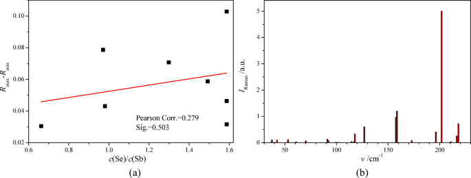
(a) Dependence of the relative value of the reflection maximum, Rmax – Rmin, in the range 221–225 cm−1 (see Fig. 8b) and the relation of the concentrations of selenium and antimony atoms c(Se)/c(Sb), (see Fig. 3c). The red direct line is the linear fit of this dependence. (b) Raman spectrum IRaman(ν) of Sb2Se3 crystal at the space group symmetry of Pnma (No. 62) calculated using CASTEP code at PBEsol exchange-and-correlation functional.
Table 3 Peak positions of Raman modes (in cm−1) of SbxSey films deposited at different source temperatures in the range 830–1000 °C and Raman modes of different crystalline substances containing Sb and se atoms49.
We have calculated the Raman spectrum of the Sb2Se3 crystal at the space group symmetry of Pnma (No. 62) (Fig. 9b) using CASTEP code50 and have found that it is very similar to the experimental Raman spectra obtained for Sb2Se3 films deposited by the same method (CMBD) on the same substrates (soda-lime glass) by several authors of the present study Ref49. Besides, the calculated frequency positions of the Raman spectrum of Sb2Se3 crystal (Fig. 9b) agree satisfactorily with the corresponding experimental Raman spectrum51 and with Raman spectra of Sb2Se3 films52.
Discussion
The increased reflection coefficients of SbxSey films for several x/y relations in the wide spectral range 30–5000 cm−1 (Fig. 8) may be caused by the over-stoichiometric antimony content, leading to the metal-like character of the radiation reflection. To verify this supposition we have performed DFT calculations of the electron energy structure of the contents Sb25Se36 and Sb26Se36, which contain one (Sb25Se36) and two (Sb26Se36) residual antimony atoms in the 1 × 3 × 1 supercell of the elementary unit cell of Sb8Se12. The optimized positions of these residual antimony atoms Sb1 and Sb2 are shown in Fig. 10.
Fig. 10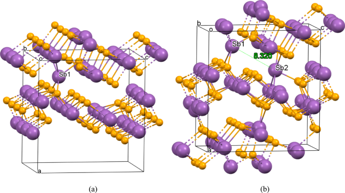
Positions of the residual antimony atoms Sb1 and Sb2 in the over-stoichiometric contents Sb25Se36 (a) and Sb26Se36 (b) corresponding to the supercell 1 × 3 × 1 of the elementary unit cell 1 × 1 × 1 (Sb8Se12). The distance d = 8.32 Å between two residual antimony atoms is indicated in the part (b) of the figure.
For the calculations of the density of states and bandgap Eg of the crystals Sb24Se36, Sb25Se36, and Sb26Se36, we have utilized the HSEsol hybrid exchange-and-correlation functional53, which is often used for the calculations of the energy bandgap Eg of crystals with high reliability. The obtained bandgap of the stoichiometric crystal Sb24Se36 is found to be Eg = 1.28 eV. In the calculated density of states of the content Sb25Se36, one separate maximum of the valence states is at the energy of 4.8 eV, which is below the Fermi level of the crystal EF = 5.414 eV (Fig. 11a). The maximum of the partial density of states of Sb25Se36 at 4.8 eV (Fig. 11b) is formed mainly by the electronic states of the residual antimony ion. In the over-stoichiometric content Sb25Se36, the bandgap is smaller, Eg = 0.923 eV, and numerous partly-occupied electronic states are in the upper part of the forbidden energy gap (Fig. 12). The electron states at the Fermi energy, E ≥ EF, and the thermally stimulated transitions of electrons from the upper donor energy states of the residual antimony atoms to the conduction band of Sb₂₅Se₃₆ can form a free electron plasma. This plasma increases the optical reflection coefficient of the Sb₂₅Se₃₆ layer in the range of 25–250 cm⁻¹ (Fig. 8b) according to the Drude relation43. The electron states just below the Fermi level EF (Fig. 12) may also be excited by photons to the lowest states of the conduction band (Fig. 11), thus forming the infrared absorption spectrum in the photon energy range of 1200–5000 cm⁻¹ (0.15–0.62 eV).
Fig. 11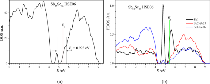
Calculated density of states (a) and partial density of states (b) of antimony selenide Sb25Se36 with one additional antimony atom in 1 × 3 × 1 supercell (Sb24Se36) of the elementary unit cell (Sb8Se12) of Sb2Se3.
Fig. 12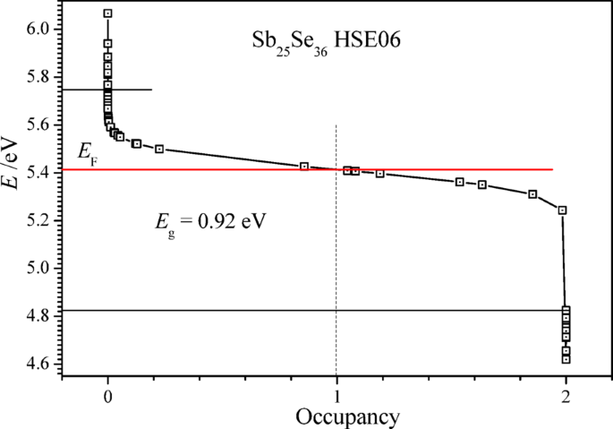
Energy of electron states E, in the range of the bandgap Eg, versus their electron occupancy calculated for non-stoichiometric Sb25Se36 (Sb + Sb24Se36) with one additional antimony atom in 1 × 3 × 1 supercell (Sb24Se36) of the elementary unit cell (Sb8Se12) of Sb2Se3.
The optical bandgap Eg of SbxSey films of thickness d was determined from the measurements of their transmittance T as a function of the photon energy hν (Fig. SD-9 of Supplementary designation). The bandgap Eg was obtained from the slope of the linear part of the dependence of the value (-hν⋅ln(T)/d)2 on the photon energy hν, corresponding to the direct optical transitions. It was found that the dependence of the bandgap Eg of SbxSey films on their content index x/y (x/y = NSb/NSe) is close to a linear one with a negative slope coefficient dEg/d(x/y) and is similar to that obtained in the previous study54 (Fig. 13a). However, the absolute value of the experimental slope coefficient |dEg/d(x/y)| = 0.292 (Fig. 13a) is substantially smaller than the theoretical one |dEg/d(x/y)| = 10.07 (13b). This is likely caused by the fact that the majority of the residual antimony atoms are placed out of the polycrystals of SbxSey films in the form of a metallic phase in SbxSey films as already seen by XRD analysis. The latter circumstance also explains the experimentally observed increase of the reflection coefficient of SbxSey films with an increase of the NSb/NSe relation (Fig. 8).
Fig. 13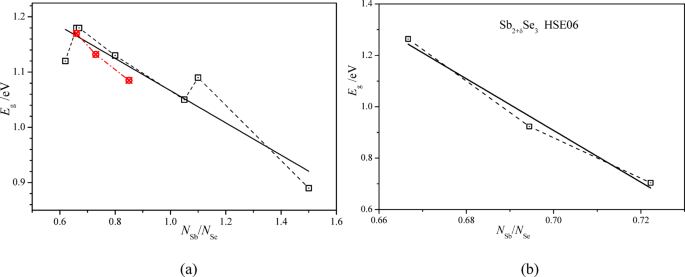
Dependences (a) of the optical bandgap Eg of SbxSey films determined by the transmittance measurements T(hν) (red points relate to the corresponding experimental study in Ref54. and (b) of the theoretical optical bandgap Eg of Sb24Se36, Sb25Se36, and Sb26Se36 crystals on their atomic content NSb/NSe.
To confirm the supposition that the majority of the non-stoichiometric antimony atoms can be aggregated outside the polycrystals Sb2Se3 in SbxSey films we have performed comparative calculations of the total energy of (a) one and two residual antimony atoms inside Sb24Se36 supercell and (b) one residual antimony atom adsorbed on the surface of Sb48Se72 supercell. In the latter case, a twice larger supercell dimension perpendicular to the surfaces of the Sb48Se72 slab was chosen to minimize the atomic interaction between atoms of two parallel slabs’ surfaces. For the residual antimony atom localized inside the Sb24Se36 supercell, the binding energy Eb(Sb) ranges from 3.10 to 3.51 eV (Table 4). For the non-stoichiometric antimony atom localized on the slab’s surfaces [100], [010], and [001] originated from the Sb48Se72 supercell, the binding energy Eb(Sb) is found to be in the range of 3.35 4.19 eV (Table 5). These results indicate that the probability of localization of the non-stoichiometric antimony atoms on the [100], [010], and [001] facets of the polycrystals Sb2Se3 in SbxSey films is greater than that inside these polycrystals.
Table 4 Total energy E for supercell contents Sb24Se36, Sb25Se36, and Sb26Se36 and binding energy Eb(Sb) for the residual antimony atom in Sb25Se36 and Sb26Se36 supercells.Table 5 Total energy E of Sb24Se36 slabs [100], [010], and [001] and one antimony atom on the surfaces of these slabs and binding energy of the residual antimony atom Eb(Sb) on the surfaces of these slabs.
On the other hand, we have found that the calculated cohesive (or binding) energies of the metallic antimony (Sb) and antimony selenide (Sb2Se3) crystals are respectively equal to Ec(Sb) = 3.12 eV and Ec(Sb2Se3) = 3.34 eV. This, in turn, indicates that the probability of crystal growth of Sb2Se3 is higher than that of the metallic antimony. These results indicate that during SbxSey film deposition, the growth of Sb2Se3 crystals is preferable to the independent growth of metallic antimony crystals. However, the growth of metallic antimony crystals becomes more probable on the surfaces of Sb2Se3 crystals due to the high bonding energy of the antimony atoms Eb(Sb) on the facets of Sb2Se3 crystals (Table 5). Moreover, in the late stages of SbxSey film deposition, the over-stoichiometric antimony atoms of Sb2Se3 crystals can move due to diffusion from the inner parts of the Sb2Se3 crystal to its surface, because of the larger binding energy of the antimony atoms on the crystal facets (3.35–4.19 eV, Table 5) in comparison to its body (3.10–3.51 eV, Table 4). These factors may promote the possibility of depositing the over-stoichiometric antimony on the facets of Sb2Se3 polycrystals in the form of a thin metallic antimony layer. In turn, such a metallic antimony layer on SbxSey films studied may be a reason for the increasing reflection coefficient in the far-infrared range with increasing their antimony content due to the free electron plasma (Fig. 8b). The proposed explanation agrees with the XRD measurements of the films studied (see Chap. 2), in which two main substances, the antimony selenide Sb2Se3 and the residual metallic Sb, were detected.
Summarizing the results obtained for Sb₂Se₃-based films, one can state that the experimental and theoretical studies of the optical properties of the films in the wide infrared range of 30–8000 cm⁻¹ can be useful for checking the necessary properties important for the photoelectric applications of these and similar semiconductor films.
In the spectral range of 500–8000 cm⁻¹ (0.06–0.99 eV), one can obtain information mainly on the possible local and distributed electron states caused by doping and structural imperfections in the films deposited by different methods. The local electron states can be detected in the form of spectral bands, which are frequently observed at relatively low temperatures. In turn, the distributed electron states are revealed as quasi-free electrons or holes, which can be fitted by the known Drude-Lorentz relation43. In the studied Sb₂Se₃-based films, both types of electron states occur. The local electron states in these films can cause the dependence of their bandgap Eg on the antimony content (Fig. 13). In turn, the quasi-free electrons or holes in the films are revealed in the increased level of the reflection coefficient for the frequencies, which are proportional to the concentration of these carriers (Fig. 8b).
In the spectral range of 30–240 cm⁻¹ (3.72–30 meV), phonon excitations in Sb₂Se₃-based films are revealed in the form of well-defined spectral peaks (Fig. 8b). The phonon spectral structure is closely related to the spatial symmetry and interatomic distances in the Sb₂Se₃ polycrystals that form the deposited films. Thus, these characteristics, when obtained for the deposited Sb₂Se₃-based films, may also be useful for the optimization of the corresponding deposition conditions.