
Suspended Si NWs with different dimensions and layouts are fabricated to evaluate the repeatability and robustness of the proposed process (Fig. 3). Figure 3a shows suspended single Si NWs with a CD of 50 nm and AR of 20, 50, and 100, corresponding to NW lengths of 1 µm, 2.5 µm, and 5 µm, respectively. Complete release is achieved across all geometries, indicating reliable transfer from preform definition to the final suspended structure. Even at AR = 100, the NWs exhibit no visible sagging, buckling, or deformation, confirming structural integrity and effective sidewall protection during DRIE. The consistent undercut observed in the array structures, characterized by typical DRIE scalloping, further confirms controlled release with limited lateral over-etching. Figure 3b shows NW arrays with identical CDs and varying ARs of 20, 50, and 100, demonstrating process uniformity and scalability. The arrays are defined with a pitch of 5 µm, consistent with the design and confirming controlled layout definition. High-magnification images reveal consistent linewidth across the arrays and robust anchoring at shared support clamps, indicating good dimensional control and repeatability. The nominal geometry is again preserved across all AR without observable deformation, reflecting effective sidewall protection during DRIE.
Fig. 3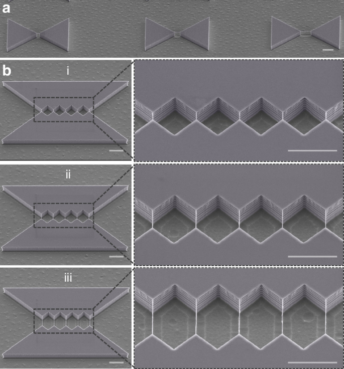
Suspended Si NWs fabricated with different geometries. a SEM images of single NWs with a CD of 50 nm and AR of 20, 50, and 100 (from left to right). b Five-NW arrays with identical CDs (50 nm) and varying AR: (i) AR = 20, (ii) AR = 50, and (iii) AR = 100. Corresponding high-magnification views highlight uniform linewidth, controlled sidewall profiles, and robust anchoring at common support clamps. Scale bar: 5 µm
The out-of-plane thickness of the suspended Si NWs is determined by the shallow Si etch step used to define the nanoscale preform (Fig. 1e). Cross-sectional TEM analysis (Fig. 1k, l) reveals a NW thickness of approximately 60 nm, which remains consistent across fabricated suspended NW structures. This confirms that the NW thickness is governed by the preform definition and is largely independent of NW length and layout. The preservation of this thickness after DRIE release further indicates that the conformal sidewall passivation effectively protects the NW geometry during etching. For in-plane dimensions, with a nominal NW CD of 50 nm, CD uniformity and line edge roughness (LER) are evaluated using top-view SEM images for AR = 20, 50, and 100 (Fig. S1 and Text S2). LER values below 7 nm are obtained across all structures, confirming consistent pattern transfer through lithography, etching, and release. The extracted values depend on SEM resolution and contrast; therefore, higher-magnification imaging could further refine the analysis.
The fabrication was demonstrated at the chip level using batch-compatible cleanroom processes, including optical lithography, PECVD/PVD deposition, plasma etching, DRIE release, and stripping/cleaning. The process does not require serial NW placement, transfer printing, individual device assembly, or manual manipulation of released nanostructures, supporting its scalability toward R&D and pilot-line fabrication. Statistical analysis is performed on the overall 20 NWs per geometry from 3 chips, using 100 sampling points per NW to estimate LER, thereby confirming dimensional reproducibility across multiple released structures. For SOI-based devices, resistance statistics from repeated measurements on single NWs and NW arrays are used to assess fabrication performance and reproducibility. Wafer-level yield qualification would require extended process-control studies beyond the scope of the present work.
The initial CD is defined by EBL in PMMA and can be influenced by proximity effects, local dose variation, resist development, and charging. This variation is transferred into the Cr hard mask, where lift-off quality, metal grain structure, and edge roughness can further affect the mask boundary. During oxide and shallow Si etching, finite mask selectivity, lateral etching, and microloading can modify the nanoscale preform geometry. Additional variation can arise during sputtered Cr sidewall passivation because local shadowing and angular deposition affect the protection thickness on the trapezoidal preform sidewalls. Bosch DRIE release can further introduce layout-dependent effects, including local etch loading, undercut variation, and scalloping. The larger apparent variation in NW arrays and SOI device layouts discussed below is therefore attributed to the combined influence of pattern density, local device geometry, SEM edge contrast, and image-analysis uncertainty. Since the final Cr and SiO₂ stripping steps do not significantly etch crystalline Si, linewidth deviation is primarily attributed to lithography, hard-mask definition, pattern transfer, sidewall protection uniformity, DRIE release, and SEM metrology.
Figure 4 presents the electrical characterization of various NW device architectures on SOI substrates, confirming their electrical functionality and suitability for sensing applications. The investigated structures comprise a single NW, a five-NW parallel array, and a suspended NW integrated within a FET configuration. Electrical measurements are carried out using an Agilent B1500A semiconductor parameter analyzer connected to a probe station. Figure 4a shows I–V characteristics of two-terminal devices, including a single NW and a five-NW array, under a voltage sweep from −100 mV to +100 mV. The nominal NW length is 2 µm, and the CD is approximately 60 nm. Both devices exhibit linear I–V behavior, confirming ohmic conduction. At +100 mV, the single NW exhibits a current of ~330 nA, whereas the NW array reaches ~1500 nA, consistent with increased conduction through parallel NW channels. Similar behavior is observed under negative bias. This response indicates uniform electrical behavior and consistent contact formation across the NWs.
Fig. 4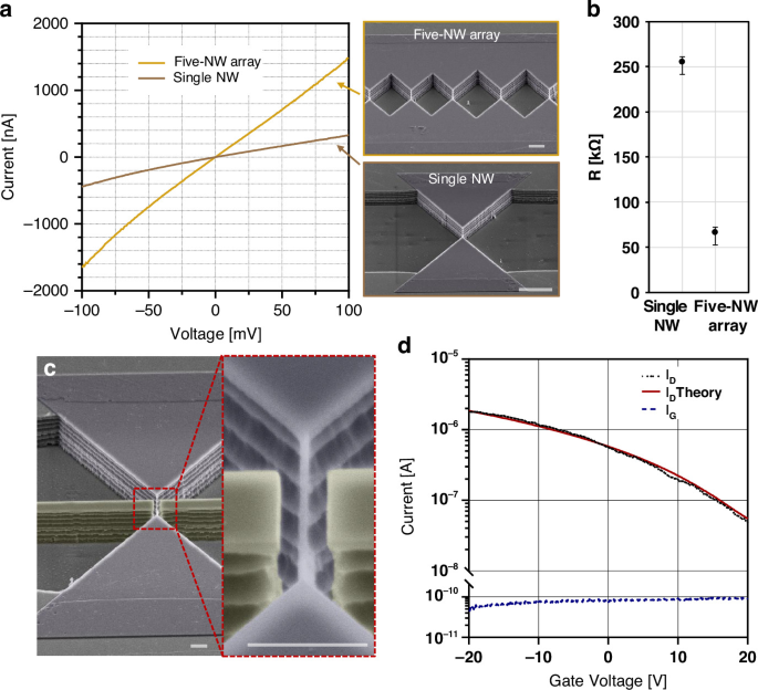
Electrical characterization of Si NW devices fabricated on SOI substrates. a Current–voltage (I–V) characteristics of a single NW and a five-NW array, showing linear ohmic behavior and increased current in the array configuration. Insets show false-colored SEM micrographs of the corresponding devices (scale bar: 5 µm). b Variation in the resistance of the NWs measured across multiple chips, indicating sufficient fabrication repeatability. c False-colored SEM micrograph of a suspended Si NW integrated with lateral gate electrodes; the close-up highlights the suspended NW channel and gate–NW spacing (scale bar: 1 µm). d Gate voltage-dependent drain current of the FET device in (c), showing depletion-mode modulation. The analytical model is plotted for comparison. The gate leakage remains two orders of magnitude lower than the drain current
Resistance values are extracted from the slopes of the I–V curves, yielding approximately 256 kΩ for the single NW and ~67 kΩ for the array (Fig. 4b). This reduction approximately follows the expected inverse scaling for five NWs connected in parallel. The measured array resistance (~67 kΩ) exceeds the ideal inverse-scaling value (~51 kΩ), indicating a deviation of about 30%. While Fig. S1 shows that NW arrays exhibit greater CD variation and higher LER than single NWs, this geometric variability alone does not account for the observed increase in resistance. The deviation is therefore attributed to additional contributions from contact resistance and non-uniform current distribution among parallel NWs. Overall, these results demonstrate that the fabricated NWs exhibit reliable and predictable electrical behavior, with only minor deviations from ideal scaling arising from contact resistance and non-uniform current distribution, confirming their suitability for device-level implementation.
Figure 4c shows a false-colored SEM micrograph of a suspended 2 µm-long NW located between the gate electrodes, separated by a well-defined air gap of approximately 120 nm on each side. A close-up view confirms that the NW is fabricated without stiction or deformation, maintaining structural integrity despite the small spacing. This configuration constitutes a multi-terminal architecture in which the suspended Si NW channel with source and drain contacts at both ends is integrated with gate electrodes, forming a junctionless FET. While preserving the mechanical functions of suspended NWs, this approach also maintains direct surface accessibility of the NW channel for post-processing and functionalization11,56. The gate electrode width is approximately 50% of the NW length.
The source is grounded, while the drain and gates are biased using independent source-measure units (SMUs). The gate voltage, \({V}_{G}\), is swept from −20 V to +20 V at a constant drain bias of 8 V to evaluate gate-induced channel modulation. The sample chuck is grounded to minimize electrostatic charge buildup. The measurement configuration and wiring scheme are shown in Supplementary Fig. S2. Figure 4d presents the resulting electrical characteristics of the suspended Si NW FET. The drain current, \({I}_{D}\), varies systematically with gate voltage, \({V}_{G}\), confirming effective electrostatic modulation of the channel. The device operates as a depletion-mode transistor. At \({V}_{G}=0\) V, the device exhibits \({I}_{D}\approx\) 600 nA, which decreases to the order of 50 nA at \({V}_{G}=+\) 20 V and increases to the order of 2 µA at \({V}_{G}=\) −20 V. This behavior is consistent with a p-type channel. Negative gate bias enhances hole accumulation, reducing channel resistance and increasing current, whereas positive gate bias induces depletion at the Si NW–air interface, reducing the effective conducting cross-section and increasing channel resistance. The observed modulation corresponds to an effective threshold voltage, VT, of approximately 24 V. The simultaneously measured gate leakage current remains close to the measurement noise floor, in the range of approximately 50–100 pA (Fig. 4d), and is several orders of magnitude lower than the drain current measured in the gate-voltage range. This confirms that the observed drain-current modulation originates from electrostatic control of the suspended Si NW channel rather than leakage through the gate path. This modulation functionality is realized entirely within a low-thermal-budget process, demonstrating that suspended Si NW FET architectures can be fabricated and operated without conventional high-temperature steps such as thermal oxidation or LPCVD.
A compact drift model is used to quantify the FET behavior. For a laterally gated Si NW channel, the standard quadratic form is given in Eq. 1
$${I}_{D}=\frac{1}{2}{K}_{p}{\left({V}_{{GS}}-{V}_{T}\right)}^{2}$$
(1)
where, \({K}_{p}=\frac{W}{L}{\mu }_{{peff}}{C}_{i}\,({{\rm{A}}}/{{{\rm{V}}}}^{2})\), is the transistor transconductance parameter. For \({k}_{p}\), \({\mu }_{{peff}}\) is the effective hole mobility \(({{cm}}^{2}/{{\rm{V}}}-{{\rm{s}}})\), and \({C}_{i}\) is the air-gap capacitance per unit area associated with gate-NW spacing \(({{\rm{F}}}/{{cm}}^{2})\). The electrical aspect ratio \(w/L\) is inversely related to the geometrical aspect ratio (AR = \(L/w\)), although it represents an effective parameter in the electrical model rather than a strictly equivalent physical quantity. VGS \(=\) VG-VS represents the voltage difference between the gate and source, while VT represents the threshold voltage of the transistor. The full model, including bias-dependent effects, air-gap capacitance, and channel-length modulation, is provided in the Supplementary Information (Text S3). The model reproduces the measured characteristics over approximately two orders of magnitude in ID, with a maximum deviation of ~10–14%, mainly attributed to series resistance and contact effects. The threshold voltage, VT, of this depletion-type FET is expressed in Eq. 2.
$${V}_{T}={V}_{{FB}}+2{\phi }_{F}-\frac{\sqrt{2{\varepsilon }_{s}q{N}_{A}\left(2{\phi }_{F}\right)}}{{C}_{i}}$$
(2)
where \({V}_{{FB}}\) is the flat-band voltage, and \({\phi }_{F}\) and \({N}_{A}\) are the Fermi potential and the doping concentration of the p-type channel region, respectively. Assuming a total trapped charge of 1 \(\times \,\)10−11 cm−2, the extracted threshold voltage VT\(\sim\) 24 V and modulation magnitudes are consistent with previously reported junctionless side-gated suspended Si NW FETs54,57,58, confirming the predictability of device behavior.
To further characterize the suspended Si NW FET, the drain-current modulation, transconductance, effective subthreshold swing, and gate leakage current were extracted from the measured transfer characteristic at VD = 8 V from Fig. 4d. The drain current decreases from approximately 2 µA at VG = −20 V to approximately 50 nA at VG = +20 V, corresponding to a current modulation of approximately 40\(\times\), or about 1.6 decades. The transconductance was extracted from the measured transfer curve using gm = dID/dVG. Because the device is p-type and depletion-mode, the extracted gm is negative; therefore, the magnitude |gm| is reported. The maximum extracted |gm| is approximately 70 nS, obtained in the ON-state region between VG = −20 V and VG = −10 V. In the near-threshold and depletion regions, |gm| decreases to approximately 5–40 nS.
An effective subthreshold swing was estimated from the depletion region of the transfer curve using \({SS}=\frac{d{V}_{G}}{d\left({lo}{g}_{10}{I}_{D}\right)}\). From the current decrease between VG = +10 V and VG = +20 V, the effective swing is approximately 17.2 V/dec. This value is referred to as the effective subthreshold swing because the present device employs a suspended, side-gated air-gap geometry rather than a conventional dielectric-gated MOSFET architecture.
The extracted threshold voltage of approximately 24 V in the current work, along with other performance parameters such as transconductance and subthreshold swing, is attributed to the electrostatic coupling of the side-gated air-gap test architecture and does not represent an intrinsic limitation of the low-thermal-budget suspended Si NW fabrication process. The lateral air-gap FET serves as an electrical validation structure rather than an optimized low-voltage sensing transistor. The FET measurement is used here to verify gate-dependent modulation of the released junctionless NW channel, while comparison with literature places the present device performance in context rather than claiming optimized low-voltage transistor operation. Lower-voltage operation could be achieved by improving gate coupling through reduced gate-to-NW spacing, replacing the air gap with a dielectric gate medium such as SiO2, using higher-permittivity dielectrics to increase gate capacitance, or adopting wrap-around/gate-all-around device geometries32,54,58,59,60. These approaches would increase the gate-to-channel capacitance and reduce the voltage required for channel depletion/modulation, hence improving the FET performance.
Such suspended Si NWs with adjacent electrodes separated by nanoscale air gaps enable several device concepts, including FETs, resonators, switches, and sensors43,52,53,54,55,60,61,62, as well as gate-all-around transistor configurations when combined with conformal coatings63. Although the suspended geometry is potentially compatible with future MEMS-style physical sensing platforms (through integration of a MEMS proof mass in the design), application-specific mechanical characterization, including MEMS-Si NW resonant frequency, electromechanical readout, noise, and any physical sensor application, the focus of this work is placed on FET and related electrical characterization and chemical sensors. Previous studies have demonstrated junctionless suspended Si NW FET architectures with lateral electrostatic control54,57,58. For example, Koumela et al. reported lateral gating in oxide-encapsulated p-type Si NWs with CD \(\approx\) 20 nm, achieving modulation at zero gate bias54. Hassani et al. demonstrated FET operation in suspended p-type Si NWs with CD ≈ 45 nm and gate spacing \(\approx\) 20 nm, with device turn-off occurring at gate voltages around −7 V57. Similarly, Bartsch et al. reported junctionless n-type Si NW FETs with CDs down to \(\approx\) 35 nm and side-gate spacing of \(\approx\) 60 nm, showing depletion-mode behavior with turn-on near 0 V and threshold voltages around −6 V under comparable bias conditions58. Collectively, these studies show that depletion-mode operation is a characteristic response of suspended junctionless Si NW FETs, with threshold voltage strongly influenced by geometry, dielectric environment, and device configuration. While similar depletion-mode behavior has been reported in suspended NW FETs, the present results demonstrate this operation in a fully suspended architecture fabricated using a furnace-free, low-thermal-budget process.
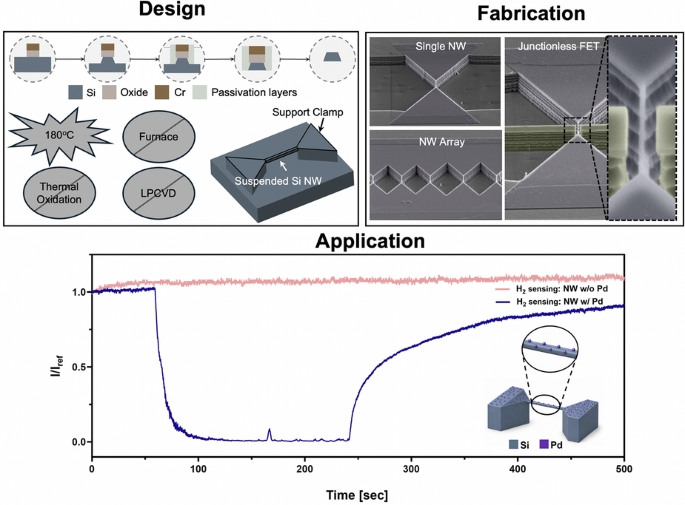
The ability to fabricate both isolated NWs and densely packed NW arrays enables complementary device configurations on the same platform. The observed uniformity, structural stability, and scalability confirm the robustness of the fabrication process for integrated device architectures. Overall, the results demonstrate the functionality of the fabricated NWs across single-NW, array, and transistor configurations on SOI substrates, supporting their use in chemiresistive gas and biochemical sensing after surface functionalization10,56,64. A central feature of the developed approach is the elimination of furnace-based high-temperature steps, such as thermal oxidation and LPCVD, commonly used in conventional suspended NW fabrication. These steps can introduce residual stress in nanoscale beams and impose stringent contamination constraints, as they require ultraclean substrates. In contrast, the present process uses sputtered Cr for sidewall passivation, enabling high etch selectivity during DRIE while maintaining a low thermal budget. The only thermal step in the process is the 180 °C PMMA soft bake, which is inherent to electron-beam lithography and does not compromise structural integrity. The comparison with previously reported processes in Table 1 highlights the substantial reduction in maximum process temperature achieved in this work.
Table 1 Process recipes for sub-100 nm NW fabrication
The low-thermal-budget process avoids furnace-based oxidation or deposition steps that can introduce intrinsic stress in suspended Si NWs. However, residual stress is not directly quantified in the present sub-100 nm NW devices. The absence of visible sagging, buckling, or deformation during SEM inspection is therefore interpreted as evidence of structural integrity after release, rather than as a quantitative measure of stress. Previous studies have shown that intrinsic stress in suspended Si NWs can arise from fabrication and surface effects, including native-oxide formation, and that its quantification requires dedicated Raman, resonant, or calibrated nanomechanical measurements44,48,65,66. Accordingly, quantitative residual-stress characterization of the present sub-100 nm NWs is left for future dedicated mechanical studies.
To further demonstrate the sensing relevance of the fabricated suspended Si NW platform, hydrogen sensing was evaluated using a single-NW device fabricated on SOI. IV characteristics were first measured without Pd functionalization, then remeasured after evaporation of a nominal 2 nm Pd layer over the suspended NW region. During the measurement, the device was biased at 100 mV, and the current was continuously monitored under repeated hydrogen exposure at a flow rate of 200 sccm.
The inset in Fig. 5a schematically illustrates the Pd-functionalized suspended Si NW device. The nominal 2-nm Pd coating serves as a catalytic functional layer for hydrogen dissociation. At this thickness level, Pd is expected to form a discontinuous nanoparticle/island-like decoration rather than a continuous metallic film, consistent with previous Pd-decorated Si NW hydrogen sensors11,67. The absence of electrical shorting after Pd evaporation, together with the preserved measurable device resistance, confirms that the Pd functionalization does not form a continuous conductive bridge across the device.
Fig. 5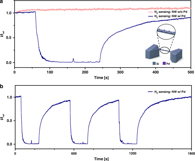
Hydrogen sensing response of a Pd-functionalized suspended Si NW device fabricated on SOI. a Normalized current response of the same Si NW device before and after Pd functionalization under hydrogen exposure. The bare Si NW shows negligible response, whereas the Pd-functionalized NW exhibits a pronounced current decrease upon hydrogen exposure and recovery after hydrogen removal. The inset shows a schematic illustration of the suspended Si NW after nominal 2 nm Pd functionalization. The Pd layer acts as a catalytic hydrogen-sensitive surface decoration. b Repeated hydrogen exposure cycles for the Pd-functionalized Si NW, demonstrating reproducible hydrogen-induced current modulation and recovery
The plot in Fig. 5a compares the normalized current response of the same Si NW device before and after Pd functionalization. The pristine Si NW shows negligible response to hydrogen exposure, confirming that the bare suspended Si NW does not provide a measurable hydrogen response under the tested conditions. In contrast, after 2 nm Pd functionalization, the current decreases sharply upon hydrogen exposure and recovers after hydrogen removal. Since the SOI device layer is p-type, the decrease in current is attributed to Pd-mediated hydrogen interactions that increase depletion/effective barrier modulation in the Si NW channel, driving the NW toward a depleted state. The repeatability of the Pd-functionalized response is shown in Fig. 5b. Repeated hydrogen exposure cycles produce reproducible current suppression followed by recovery toward the baseline after hydrogen removal.
The sensing performance of the Pd-functionalized suspended Si NW was further quantified from the transient current response. response can be defined via Eq. 3:
$${Response}\,\left( \% \right)=\,\left[\frac{{I}_{{air}}-\,{I}_{H2}}{{I}_{{air}}}\right]\times \,100$$
(3)
where Iair is the baseline current before hydrogen exposure and IH₂ is the minimum current during hydrogen exposure. Under the tested hydrogen condition, the Pd-functionalized device exhibits approximately 95–99% current suppression, whereas the pristine Si NW shows a negligible response. The response time, defined as the time required to reach 90% of the total current decrease after hydrogen introduction, is estimated at 20–30 s. The recovery time, defined as the time required to recover 90% of the current change after hydrogen removal, is approximately 200–250 s. The maximum measured current during the test is approximately 67 nA at an applied bias of 100 mV, corresponding to a maximum electrical operating power of approximately 6.7 nW. These results confirm that Pd functionalization enables a repeatable hydrogen response in the suspended p-type Si NW at sub-10 nW-level operating power.
This confirms that the fabricated suspended Si NW platform remains electrically functional after Pd evaporation and can be converted into a hydrogen-sensitive device through a simple low-temperature post-fabrication functionalization step. Raw data for hydrogen sensing before and after Pd functionalization are provided in Supplementary Figs. S3–S5.
Further simplifications for the Si NW fabrication can be achieved by, for example, replacing positive-tone PMMA with negative-tone hydrogen silsesquioxane (HSQ) resist and thereby eliminating the need for a metallic hard mask. Because HSQ converts to a SiO2-like material upon exposure, this approach could eliminate both the initial PECVD oxide layer and the intermediate oxide layer used in the current passivation scheme. Such strategies have been demonstrated in prior studies37 and could further streamline the fabrication sequence.
An alternative passivation approach would be to replace sputtered Cr with SiO2 deposited by atomic layer deposition (ALD). Compared with sputtering, ALD provides highly conformal coatings on high-aspect-ratio nanostructures, potentially improving uniformity and reproducibility for sub-50 nm NWs. In addition, ALD films can offer higher density and improved dielectric quality compared with PECVD oxides. For SOI-based integration, this approach could also eliminate the need for separate metal-pad protection during wet etching, thereby simplifying process integration.