
Key Takeaways
The parallelism in AI accelerators enables low latency but complicates failure isolation.
HBM can account for 50% of package cost, so known-good stack assurance is critical.
DFT and test cooperate to solve final test, singulated die test, SLT, and in-system test for data centers.
AI accelerators are used for everything from training large language models to making predictions based on LLMs (inferencing). They are used in real-time processing of sensor and camera data in autonomous vehicles, AI edge applications in smart phones, cameras and drones, and even for speeding up vaccine development.
But testing AI systems is a whole new ball game. It involves testing of high-speed interfaces, multiple processors, and a deep memory hierarchy. It also includes optical interfaces, which must be tested at the bare die, stacked module (HBM), final test, system-level tests, and in-field testing. This multi-die, multi-interface testing requires innovations in DFT and testing methods, including the implementation of streaming scan and the addition of more in-line stress tests and post-singulation module tests to capture all potential failures.
As package size escalates, new handling equipment and larger JEDEC trays will be needed. Test engineers are also confronting new failures at advanced nodes, at hybrid bond interfaces, inside TSVs or at bump interfaces, and at the silicon interposers. Testing is the most critical aspect of the AI journey. It needs to catch failures all the way from wafer probe to in-system at data centers.
“On the positive side, AI accelerator compute engines allow us to test against a more focused and predictable set of workloads because we know the kinds of operations they will execute,” said JohnDavid Lancaster, AI hardware research engineer at IBM Research. “On the more challenging side, these engines typically use a variety of precision formats, which can complicate establishing bit-precise expected results. Additionally, starting and stopping inference workloads can introduce large transient power swings, and thus stress the power integrity circuitry on the accelerator, which can result in failure during operation if not characterized properly.”
AI testing begins with understanding the device under test (DUT). “In these AI systems, there’s usually a single compute core that gets replicated tens or thousands of times on the same die, so it’s more of a homogeneous design compared to say, a CPU, which is heterogeneous and you’re testing the kitchen sink,” said Daniel Simoncelli, business development manager for the P93k product line at Advantest. “For AI, which is running large language models, your software stack is bespoke, and you’re going to stress the part to see whether it computes at the right coefficients. At the same time, you are testing billions of transistors. So the complexity comes from just the sheer amount of scan contents that you need to pipe into these devices.”
Thermal and power management issues are a big deal at system-level test. “Current densities for AI accelerators are high because every package in the platform requires 300 watts to 2,000 watts,” said Vineet Pancholi, senior director and manufacturing test technologist at Amkor Technology. “Precise layout of the chiplets for thermal isolation is a key architecture decision for the package design. During testing, thermal hotspots on critical areas of each die can impact both its performance and the performance of the adjacent die. Core gated test vectors allow thermal management during wafer sort, final test, and system-level test, while thermal interface material (TIM) and custom air and liquid cooled heads are employed to enable successful production test insertions.”
What is an AI accelerator?
An AI accelerator is not a single device. It’s a collection of chiplets that employ thousands of cores, along with HBM and SRAM, to provide massive parallel processing for algorithms. This differs from CPUs containing 2 to 8 cores, which handle requests sequentially and have very different workloads.
CPUs can be general-purpose, but AI accelerators tend to be designed for specific tasks. Neural processors (NPUs), for example, conduct deep learning, while tensor processor units (TPUs) excel at parallel matrix multiplications and tensor operations, the core mathematical operations in neural networks.
GPU-based modules were the first AI accelerators (and remain so for gaming and graphics processing) due to their ability to perform parallel computing while prioritizing very low latency operations. But unlike GPUs, AI accelerators prioritize high-bandwidth transfers into and out of memory, resulting in faster computations and less electricity use.
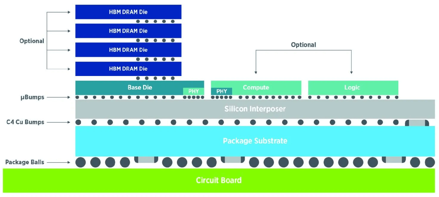
Fig. 1: Validating and testing die-to-die interfaces is critical in 2.5D and 3D packaging architectures. Source: Teradyne
There are the two main types of data center modules. “The AI module is a heterogeneously integrated advanced package consisting of one or more GPUs plus an HBM stack, high-speed serial interfaces, and co-packaged optics on an interposer. The second type is a switch plus high-speed interfaces and CPO on an interposer,” explained Jeorge Hurtarte, senior director of product marketing, Semiconductor Test Group at Teradyne. “The AI data center module is more than just one xPU, which has a maximum size of 26 mm x 33mm. These modules are in the range of 100 mm x 100 mm today and soon will be 150 mm x 150 mm, so now you have to think about testing this as a system.”
Maintaining signal integrity is a big concern when testing die-to-die interfaces. “The 2.5D and 3D packaging creates significant signal integrity and noise isolation concerns at the high-speed interfaces between chiplets,” said Quoc Phan, technology enablement manager for 3D-IC DFT and yield at Siemens EDA. “Standard fault models are simply inadequate to detect defects arising from these complex inter-die connections or within the advanced package itself, which necessitates developing specialized interconnect tests and monitors. These inter-die connections also directly impact DFT pattern delivery, raising the need for innovative DFT methodologies to efficiently create and deliver test data between dies through high-speed interfaces like UCIe.”
Despite these differences, the silicon testing priorities have not changed. “The primary testing priorities remain for achieving the highest test quality at the lowest test cost,” said Sri Ganta, principal product manager at Synopsys. “However, additional test needs arise, targeting advanced technology nodes, thermal and power stress, multi-die systems, and in-field/in-system operation.”
For AI modules, on-chip monitors are becoming more important. “The need for an end-to-end optimization becomes a necessity. There is no way anymore to make the best chip ever, and then the best system ever, and then the best rack ever, and then build a data center out of all of these, because there is too much performance and power left on the table,” said Shai Cohen, CEO of proteanTecs. “The whole point now is to make sure that for every workload, and even every couple of clocks, we need to optimize such that the overall power consumption is the lowest and the overall performance is the highest.”
The new era of multi-die testing also calls for increased collaboration among different companies. “The production complexity is staggering — coordinating substrates, base dies, third-party components, various packaging technologies, OSAT configurations, and test systems across multiple suppliers,” said John Kibarian, CEO of PDF Solutions. “While there are precedents when the semiconductor industry came together to solve formidable engineering challenges, chiplet production at scale will require even deeper collaboration levels as system companies increasingly integrate components from diverse suppliers. This orchestration must operate during initial bring-up, and throughout ongoing production, with the agility to reconfigure quickly for different product variants.”
This new scope further places a greater emphasis on innovation in design-for-test. “Testing AI ‘chips’ is such a cutting-edge challenge in semiconductor engineering today,” said Phan. “The extreme architectural complexity and massive parallelism of AI modules present great challenges.”
Scan testing now streams
For its part, scan testing (also known as structural testing) has sped up significantly to address new priorities. It’s used to catch manufacturing defects amongst millions of solder bump connections, such as opens and short circuits.
A downside to the parallel architecture of AI systems is that when a circuit does fail, it’s harder to pin down. “If some devices are failing during yield ramp, the diagnostics are a little bit more complicated, because if you get a failing bit on the test or a failing pattern, you don’t know which of the many thousands of cores in the chip has failed,” said Advantest’s Simoncelli. “So the tooling on the tester side needs to become aware of that scan network to be able to map those failing test sequences. To speed up this process, we’re looking at high-speed interfaces like PCIe. What’s neat is that suddenly, moving the test content between different insertions gets a little bit easier, because now wafer sort, final test, and SLT are all speaking the same language.”
How much easier depends on what exactly is being tested. “This massive memory usage, coupled with the large scale of the architecture, creates difficulties for controllability and observability during manufacturing test,” said Siemens EDA’s Phan. “From a DFT standpoint, generating, delivering, and applying test patterns becomes incredibly complex. The huge pattern size required to adequately cover such a vast architecture can be enormous, leading to extended test times. Furthermore, the concurrent activity across so many cores and memory interfaces means that DFT power management during testing is a critical concern, as power consumption can spike significantly.”
HBM testing’s evolution
“Due to the thousands of compute cores and deep memory hierarchies, AI systems rely on both on-chip SRAM and external DRAM, which need to transfer terabytes of data per second,” said Phan. “This massive memory usage, coupled with the large scale of the architecture, creates difficulties for controllability and observability during manufacturing test. From a DFT standpoint, generating, delivering, and applying test patterns becomes incredibly complex. The huge pattern size required to adequately cover such a vast architecture can be enormous, leading to extended test times. Furthermore, the concurrent activity across so many cores and memory interfaces means that DFT power management during testing is a critical concern, as power consumption can spike significantly.”
HBM consists of a stack of DRAM dies, typically up to 12 today. Those dies communicate through a base logic die, which recently replaced the DRAM base die. “The base die does all the checking of the memory stacked on top of it,” Simoncelli said. “And then another test is typically performed after singulation, because they’re very fragile and expensive packages. HBM can account for over 50% of the cost of the entire package, so it’s important to detect minor changes in the vertical structure, and you want to catch potential failures as early as possible. For this reason, customers are looking at another insertion. Some call it partial assembly test. Others call it singulated die test. But that is coming in the next year or so.”
On-die monitors, or agents, can be positioned on die edges to detect flaws after the sawing process. “Let’s say you want to measure in a high granularity process,” said proteanTecs’ Cohen. “Some of these agents need to sit on the edges. Yes, that may be the difference in between multi-die and regular die, wherein multi-die there is higher importance to provide visibility into the edges so that you know what’s going on in between the dies.”
As HBM manufacturers SK hynix, Micron, and Samsung go from HBM3 and HBM3E to HBM4, a key goal is packing more DRAM die — and therefore more memory capacity — into a limited stack height of less than the thickness of one silicon wafer, or 775 microns (including the base die). This standard thickness was relaxed for HBM4 from the 720 micron stack limit for HBM3/3E.
HBM4 manufacturers are expected to still use microbumps to connect each of the 16 DRAM dies, and thereafter hybrid bonding. The next generation is expected to contain 20 DRAM dies plus the base die. The high number of signal lanes needed to achieve high bandwidth means each new generation features a larger count of more densely packed through-silicon vias (TSVs), which shrinks the microbump pitch and size to about 20 to 30 microns.
“To offer high bandwidth with reduced latency, HBM memories feature very wide interfaces (1K wide, 2K wide, and moving to 4K bits wide),” said Faisal Goriawalla, principal product manager of Synopsys. “To increase capacity, the HBM standards are offering increased stack heights of 12-high, 16-high and moving to 20-high. This increases the interconnect density and number of TSVs routed through a memory stack, which means shrinking the external bump pitch as the total number of microbumps increases significantly. For the DRAM vendors, this translates to thermal, power distribution network, wiring, reliability, and TSV capacity challenges.”
But which party is responsible for HBM yield? “The DRAM vendor will ship known good die memory to the ASIC vendor/OEM partner,” Goriawalla said. “But what happens after assembly and packaging? For example, how can the OEM/system partner test for stuck-at faults on the interconnect during final test? Given the tight pitches and the large number of high-bandwidth interconnect signals between HBM memory and xPU (with several such HBM modules), it is challenging for the OEM/system integrator to comprehensively test DRAM post-packaging via ATE.”
He also emphasized the tradeoff between test time and test coverage. “Even an 8G DRAM memory can take a couple of seconds to test comprehensively on ATE. So it becomes important to have user capability to trade test time versus coverage so that detailed physical failure analysis (PFA) need only be performed if it’s warranted.”
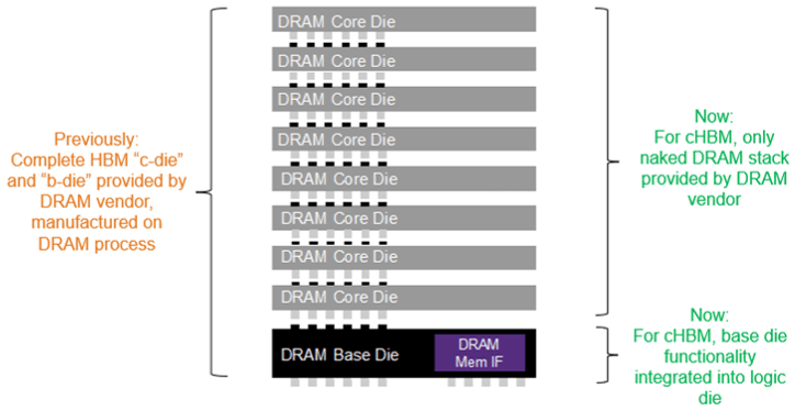
HBM testing doesn’t end with system-level test, though. In-system test is required to account for aging-related failures in data centers. “During a service/scheduled downtime, the user may want to perform specific rowhammer types of tests to detect marginalities or latent sensitivities in the DRAM to pre-empt catastrophic failures,” Goriawalla explained. “And to make testing even more ‘interesting,’ for emerging approaches such as custom HBM, the HBM base die is now developed in a logic process (rather than provided by the DRAM manufacturer in a DRAM process). This allows more design partitioning flexibility to the SoC designer, but it increases the testing complexity burden for known-good stacks and known-good packages.”

Fig. 2: In custom HBM (cHBM), testing is more challenging because DRAM base die is now fabricated using a logic process. Source: Synopsys
For all the reasons stated above — methodology/access, test time, different use case scenarios for test, emergence of custom HBM — HBM testing is a significant challenge and bottleneck, and therefore an important consideration for 2.5D IC design.
Test accessibility
About 15 years ago, leading device makers, test companies, and OSATs realized that the lack of accessibility to some dies in multi-die packaging was going to be a significant problem. That was the impetus behind developing the IEEE standard 1838. This standard is designed to enable stacked die to communicate with testers, and to use a new DFT architecture to communicate between and within non-contacting dies in a stack.
Despite all the differences with AI subsystem testing, the industry has portability with existing test methodologies. “Testing these AI packages is different than monolithic xPUs because of the lack of test access for die-to-die interconnects within the package,” said Scott Carroll, senior director of Test Business Development at Amkor. “However, all of the xPU logic test concepts, including ATPG (automatic test pattern generation), scan, structurally based function test, etc., compliant with IEEE 1838 and developed through EDA workflow for xPUs, apply well to AI modules.”
Chiplet-level logic implementation standards have helped in multiple ways. “From a DFT standpoint, UCIe allows production test simplification with redundancy repair, width degradation, and lane reversal (key features of the physical layer, PHY),” Carroll said. “Optional features may also allow TX/RX differential eye width and height verification. To comply with lower latencies between the accelerator and the memory, AI workloads continue to command higher I/O data rates (32 Gbps to 64 Gbps). Near-end and far-end loopback DFT are used together to ensure adequate test coverage.”
Carroll noted that the industry continues to collaborate to optimize DFT. One such team is the IEEE P3405 group, which may be proposing a die-to-die interconnect test generator and checker block, as well as other test methods.
Another challenge is validating the connectivity between processor units (xPUs) and HBMs, which today are connected through microbumps to the silicon interposer. “There are some significant challenges in electrically ensuring that connectivity,” said Advantest’s Simoncelli. “You have optical inspection of the bumps, but that isn’t an electrical test. So you do that electrical test once the processors are connected to the package.”
Pin access is yet another challenge. “With advanced packages, we don’t have access to all of the pins, so we need to have access to DFT interfaces to test it as a system,” said Teradyne’s Hurtarte. “For example, the streaming scan network (SSN) from Siemens can help the ATE and speed up scan test. So you have to have the right interfaces to test it as a system.”
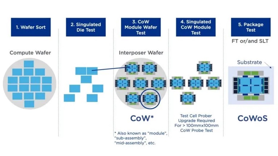
Fig. 3: Chipmakers are exploring additional test insertions, especially following dicing/singulation steps. Source: Teradyne
“The other important interface is optical because one critical way to reduce power consumption is by transitioning from copper to silicon photonics. We recently brought to market a production ATE system for optical testing, replacing the rack and stack, lab-based systems of the past,” added Hurtarte.
Lancaster explained IBM’s approach to SLT. “During manufacturing, we stress the chip in its card-level configuration as aggressively and as much as possible. This includes running AI workloads at voltage/temperature biases with the goal of lowering the operational margin that we have against failure during test, giving us confidence in the robustness of the chip and card when deployed in the field.”
This level of testing requires a multi-layered approach. “In these phases, we enable a full suite of diagnostic modes, including checking all bit-precise results, verifying our most intense AI models from a hardware perspective,” said Lancaster. “Since enterprise customers require extremely low field failure rates, our testing process includes extensive hardware validation testing, from module-level tests to full system-level integration and stress testing. This multilayer approach ensures reliability of both the silicon and the platform it integrates into.”
One rule-of-thumb is that testers should be capable of exerting twice the voltage stress level as should be required for operation of parts in the field. “To stress all of the components on our chip, we have a suite of hardware validation tests that target specific blocks and interfaces on the chip. We run these tests at various frequencies, voltages, and temperatures while enabling full diagnostic checking,” said Lancaster. “Additionally, these tests are queued via hardware-specific testers designed to provide deeper visibility and higher stress levels than typical customer workloads. This ensures that issues are caught early, under more extreme conditions than the end user will typically encounter.”
Conclusion
The AI accelerator journey is just beginning, but already much has been learned on the testing side.
“It’s a long road ahead for AI IC production testing,” said Amkor’s Pincholi. “However, after the first wave of products moves through assembly and test, we’ll gather additional data and insights to better understand missed opportunities and key learnings. We’ll use this experience to strengthen and streamline our approach for future AI products.”
The next part of this series will further explore the DFT and testing challenges posed by the introduction of AI accelerators.
Related Articles
Mission-Critical Devices Drive System-Level Test Expansion
SLT walks a fine line between preventing more failures and rising test costs.
AI In Test Analytics: Promise Vs. Reality
Turning big data into reliable yield insight requires more than good models.
Optimizing DFT With AI And BIST
AI-driven automation, tighter design-test collaboration, and evolving BiST techniques are redefining DFT strategies.