It is beginning to look like that the period spanning from the second half of 2026 through the first half of 2027 is going to be a local maximum in spending on XPU-accelerated systems for AI workloads. And as the number and type of XPU accelerators is growing to fulfill that compute demand from the hyperscalers and cloud builders and now for the biggest AI model builders like OpenAI, the demand spike for HBM stacked memory is no doubt going to outstrip supply.
Couple this with the increasing difficulty of manufacturing HBM memory as the height of the stacks, the density of the DRAM, and the bandwidth delivering all increase, which has resulted in ever-decreasing yield that is inevitable and unavoidable and the AI compute segment is going to be squeezed by too much demand chasing too little supply.
Something has to give, and that something in the Nvidia product line is now called the “Rubin” CPX GPU accelerator, which is aimed specifically at parts of the inference workload that do not require high bandwidth memory but do need lots of compute and, increasingly, the ability to process video formats for both input and output as part of the AI workflow.
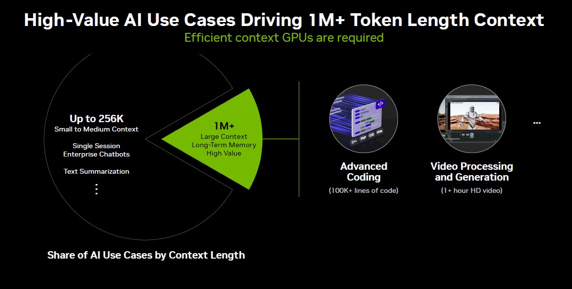
The target of the Rubin CPX GPU is large context length AI inference workloads. Nvidia reckons that code generation and analysis and video processing and generation workloads have context windows of 1 million tokens or more, and it gets very expensive to support such long contexts on expensive GPUs loaded up with very expensive HBM memory stacks. These are high value workloads, but they are expensive to support:
It looks like about 1/6th of the AI use cases have a need for such large context windows, and code generation and analysis in particular is one of the early and clearly successful use cases for GenAI, so Nvidia wants to remove some economic barriers to adoption.
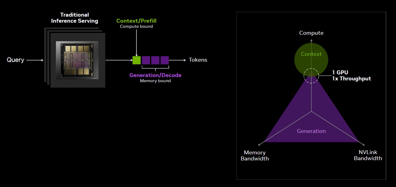
Here is the deal. If you try to do long context processing on a single GPU that has a lot of compute as well as memory bandwidth and capacity, you won’t have the right balance for each part of the context processing (called prefill) and the generation (called decode) parts of the inference. The memory bound generation operation can only proceed once the compute bound context processing is done. Like this:
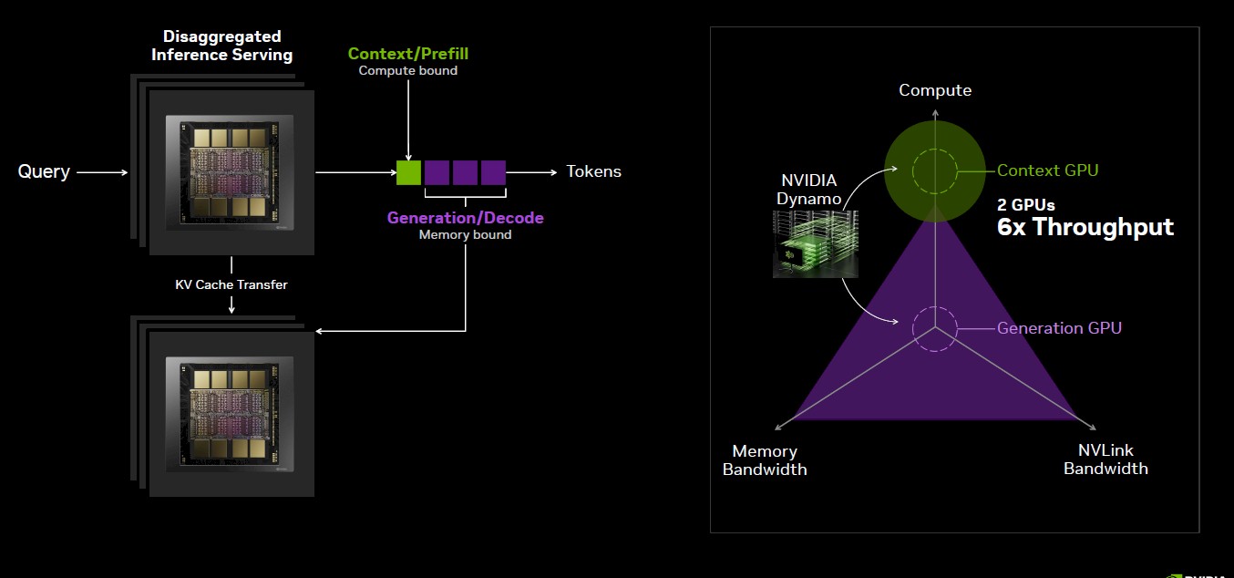
But, you can disaggregate the context processing from the generation, and in this scenario you have a Rubin GPU CPX chewing on the context and a Rubin GPU doing the generation of tokens, with a KV cache linked the two and even allowing you to store KV functions to speed up token generation because you are not reprocessing the whole token context with each token that is generated. So, says Nvidia, you can use two GPUs and get 6X the throughput for long context AI inference.
It is pretty obvious that 6X the throughput is great for only adding 2.25X more compute, which you will see is the ratio for the rackscale systems Nvidia is designing for late next year.
Not Just A Cheap Chip, But Disaggregated Inference
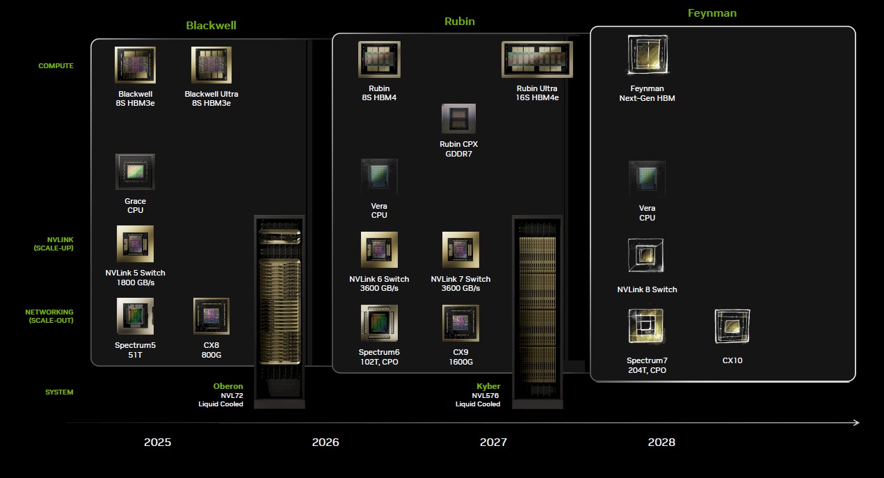
Nvidia has made special, lower-cost GPU accelerators for the datacenter from its gaming and workstation GPUs for many years, so it is no surprise that a cutdown variant of the future Rubin architecture that looks more like a gaming or workstation GPU would be used for inference. But this time, with the Rubin CPX, the technology strategy is a little bit different, and it looks like it is a bit cleaner architecture-wise if you can take the images that Nvidia is using for the future Rubin R100/R200 GPUs already on the roadmap and the new Rubin CPX just added to it somewhat literally.
In the past, Nvidia took one of those gaming or workstation GPUs and equipped it with passive cooling so it could fit into a server chassis and be cooled like the other components, and then it might have deactivated certain graphical functions and slapped a datacenter name on it. The GPUs used in inference machines were considerably architecturally different from the “real” workhorse datacenter GPUs. This was the case with the inference engines based on the “Turing” TU102 and TU104 chips from 2018, the “Ampere” GA102 and GA104 kickers from 2020, and the “Ada Lovelace” AD102 and AD104 follow-ons from 2023. We have not done a deep dive with the GB202 “Blackwell” RTX GPUs used in the RTX 5000 series accelerators, but the same strategy holds.
Moreover, all of these accelerators and the forthcoming Rubin CPX make use of GDDR frame buffer memory used with graphics cards instead of HBM memory. This memory provides more bandwidth than plain vanilla DDR DRAM used for server CPUs but a lot less than the HBM memory used in datacenter GPU accelerators.
But with the Rubin CPX, the architectural differences between the workhorse R100 and R200 GPUs in the datacenter (and the eventual R300 that will double its performance a year later) and the CPX devices will be less. The Rubin CPX will use GDDR memory with lower capacity and lower bandwidth, which will be used to get the price down and also the unit volumes up.
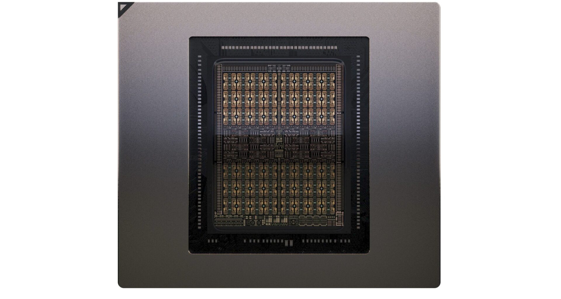
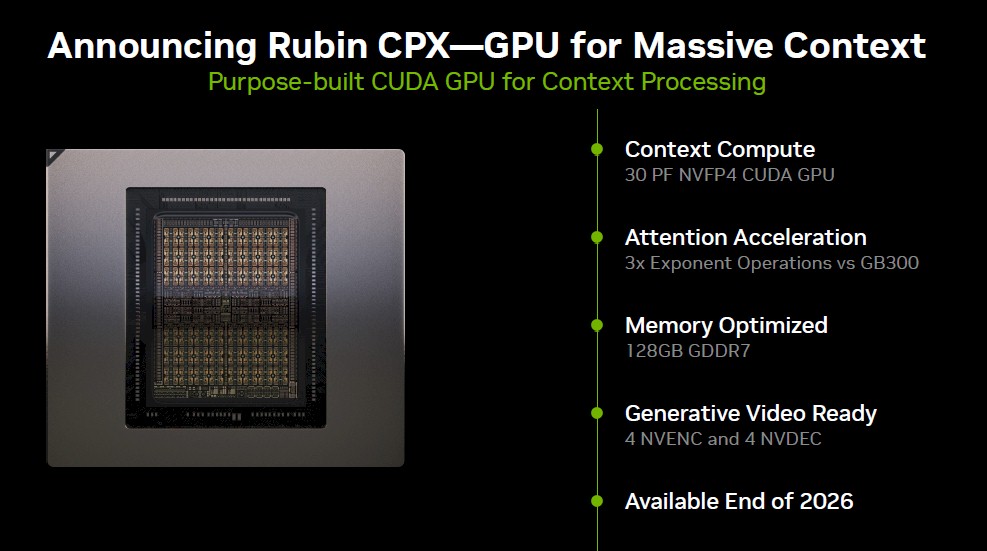
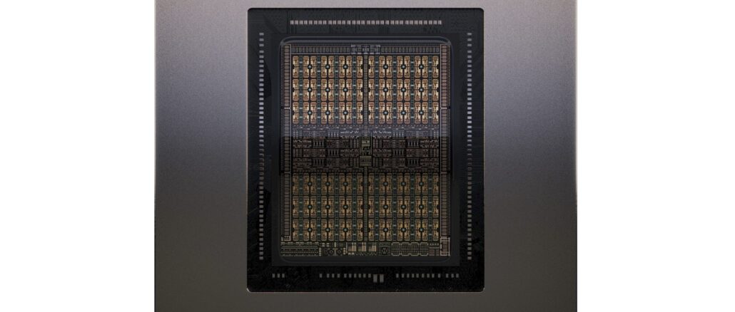
Here is what the Rubin CPX looks like:
The Rubin CPX chip is rated at 30 petaflops of floating point oomph at FP4 four-bit precision – what Nvidia has been starting to call NVFP4 to distinguish it from other FP4 formats like the MXFP4 format upon which it is derived as well as the distinct FP4 used with AMD’s Instinct MI series GPUs and the experimental NF4 variant, among others.
According to the roadmap presentation of Nvidia co-founder and chief executive officer Jensen Huang back in March at the GTC 2025 conference, a two chiplet Rubin socket in 2026 will be rated at 50 petaflops FP4, and a four chiplet Rubin Ultra socket in 2027 will be rated at 100 petaflops FP4. So, it looks like there will not be a bifurcation of performance with Rubin with FP4 and FP64 performance as we saw with the variations of Blackwell. (The question is whether or not Rubin will have good FP64 performance at all.) Given this, it sounds like Nvidia is putting only one Rubin chiplet in the Rubin CPX package and boosting its clocks by 20 percent to get to that 30 petaflops at FP4 precision.
It is a bit of a wonder that there has not already been a Blackwell Ultra CPX chip launched, given the intense pressure of bringing the overall cost of inference down right now. This is especially true now that the Blackwell Ultra B300 chip is ramping its shipments. Here’s why. The Ultra-class GPU in the Blackwell family (the B300) is aimed at inference workloads, and in fact has its FP64 floating point performance deprecated so more lower-precision FP4 computing can be added to the pair of GPU chiplets that make up the Blackwell Ultra package. The B100 and B200 are aimed more at traditional HPC and AI training workloads but obviously can do inference, too, but the B200 only pushed 10 petaflops at FP4 compared to 15 petaflops at FP4 for the B300.
It is amazing to us that Nvidia is willing to wait until the end of 2026 to solve this inference problem by disaggregating GPUs and aiming different ones at different parts of the workflow. (More on this in a second.) The point is, a single B300 GPU chiplet running at 7.5 teraflops FP4 or a single B202 chiplet used in the RTX 6000 Pro datacenter cards rated at 4 petaflops FP64 that were equipped with the video encoder/decoders is better than waiting a year. Getting the HBM memory controllers out of the package and getting the GDDR memory controllers and video encoders into the package must be trickier than we think it is with the CPX. Nvidia must want to sell a lot of RTX 6000 Pro datacenter cards in the next year.
Perhaps the thing that makes this CPX approach killer is the attention acceleration that is coming with the Rubin architecture, which Ian Buck, vice president of hyperscale and HPC, mentioned in passing during the reveal of the Rubin CPX compute engine at the AI Infra Summit in Santa Clara this week. “We have tripled down on the attention processing,” Buck explained in his keynote, referring to the rate of attention processing that can be had with the Blackwell B300 GPU, which presumably is no slouch. “Attention is the building block of many of the models we have today, and we have actually added attention acceleration cores to the chip.”
The lack of such cores in Blackwell may be another reason why Nvidia decided to wait until Rubin to make a CPX. And the good news is that this attention process in the AI model – literally finding the key words for the input context and figuring out what is important – is relatively compute intensive but not particularly memory bandwidth intensive. (Attention processing is kind of neutral when it comes to memory capacity.)
The differences in the Rubin chips is stark when it comes to memory capacity and bandwidth, and therefore so should the costs be. The Rubin CPX socket has 128 GB of GDDR7 graphics memory, which is a lot less than the 288 GB of HBM3E used in the Blackwell Ultra socket, the 288 GB of HBM4 expected in the Rubin socket, and the 1,024 GB of HBM4E used in the Rubin Ultra socket. Buck gave some hints about the cost differential in his presentation.
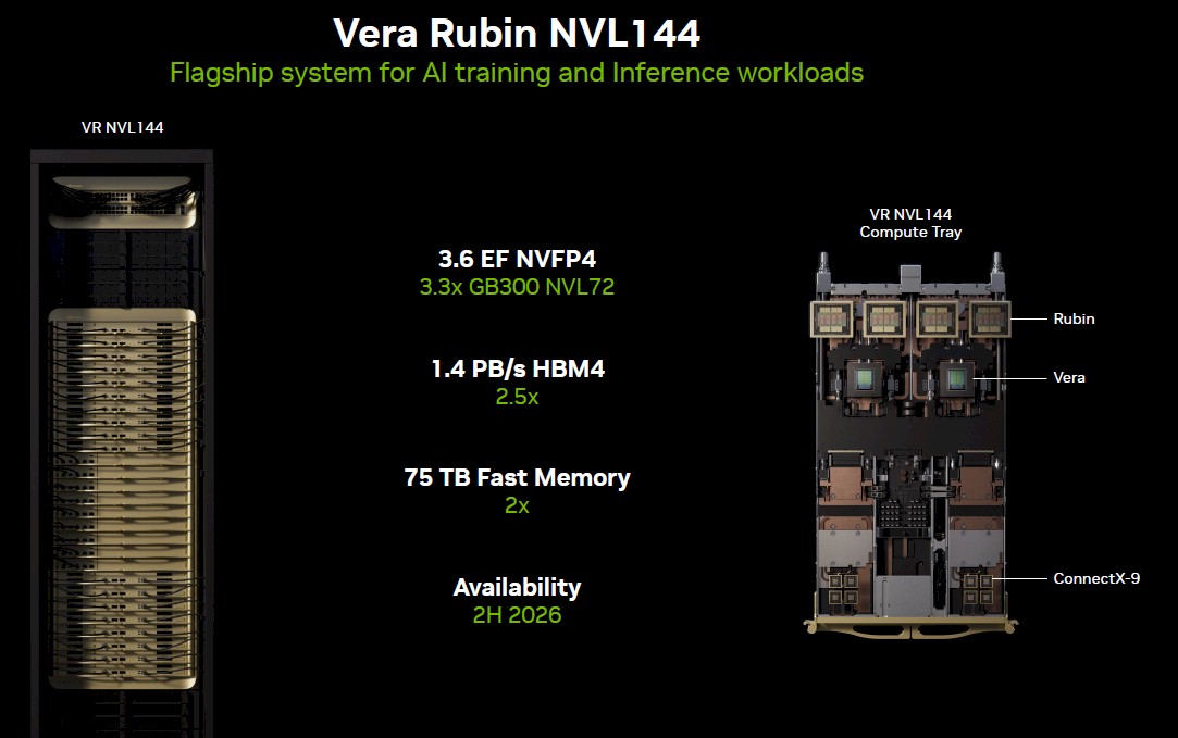
Here are the feeds and speeds for the Vera Rubin NVL144 rackscale system:
The HBM4 memory used in these devices will deliver somewhere just shy of 10 TB/sec of bandwidth per socket against that 288 GB of capacity, while the 128 GB of GDDR7 memory might be pushing something shy of 2.1 TB/sec depending on its speed and arrangement. (A rack of Vera Rubin has 1.4 PB/sec of memory bandwidth on the 72 accelerator sockets, and a combined Vera Rubin with 144 Rubin CPX accelerators added has 1.7 GB/sec of memory bandwidth. If you do all that math backwards you get 2.1 TB/sec of bandwidth per Rubin CPX socket.)
By the way, as far as we know, a rack of Vera Rubin has 20 TB of HBM4 memory, so this “fast memory” stat shown in the specs above is likely the combination of LPDDR5 memory on the “Vera” CV100 CPU plus the HBM4 memory on the Rubin GPU. That suggests the Vera CPU will have 1.5 TB of memory, more than 3X what the current “Grace” CG100 CPU has. Add it all up and the Vera Rubin rack is rated at 3.6 exaflops at FP4 precision, which is 3.3X that of the GB300 NVL72 system that Nvidia is just starting to ramp up now.
It pays to wait if you can. Clearly.
But wait, there’s more. Take that same Vera Rubin rackscale system and now interpose eight Rubin CPX inference context processors between the ConnectX-9 network interfaces and the Vera-Rubin processing complex and see what happens:
Now there is an additional 4.4 exaflops of FP4 compute in the rack, that extra 300 TB/sec of aggregate bandwidth, and another 25 TB of additional fast memory (128 GB times 144 Rubin CPX devices). And here, Buck laid down some numbers: For every $100 million of money invested in racks of Vera Rubin CPX machinery, the machine could drive $5 billion in revenue for tokens input and output as part of an application or API stream. (Presumably that is over a four year span, but Nvidia was not precise.) Buck did not give similar cost and revenue numbers for a Vera Rubin rack without the Rubin CPX accelerators, which would have been useful. For long context processing, clearly this CPX-accelerated setup is better, so it might be something like for every $80 million invested, you drive $2.25 billion in revenues over four years.
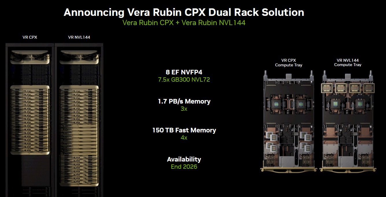
Now, you don’t have to just disaggregate the inference workload inside of each node in a rackscale system. You can use a node as your unit of compute and have distinct Vera Rubin and Vera Rubin CPX nodes. Like this:
You get another extra 50 TB of “fast” memory from doubling up the Vera CPUs across the double racks if you do it this way, and you don’t have to link these together using NVLink switches, either. From the looks of it, you could have a ratio of 288 Rubin CPXs to 144 Rubin chiplets and 72 Rubin sockets if you wanted to do that – there looks to be room in the Vera Rubin CPX rack.
We wonder if the Vera Rubin CPX racks would be good for processing inference for smaller models, not just the long context for code and video generation. And we look forward to seeing the pricing on all of this next year to see how it all plays out.
Featuring highlights, analysis, and stories from the week directly from us to your inbox with nothing in between.
Subscribe now
Related Articles

