We live inside a storm of invisible signals. Phones, Wi-Fi routers, 5G networks, smartwatches, and medical sensors constantly send and receive electromagnetic waves.
While this wireless traffic powers modern technology, it also creates a serious side effect, electromagnetic interference (EMI). These unwanted signals can confuse or disrupt delicate electronics, especially in medical devices, wearable sensors, and flexible displays, where failure is not an option.
Until now, blocking this interference has required thick metal layers that are rigid, heavy, and opaque. That makes them unsuitable for transparent or bendable electronics.
However, a team of researchers has now shown a unique solution in the form of an ultra-thin, flexible, see-through film that can block almost all unwanted electromagnetic radiation while remaining light, transparent, and scalable for real-world use.
“This is the first time anyone has overcome the longstanding trade-off between electrical conductivity and optical transparency in metallic nanowire networks. After our laser post-treatment, both the conductivity and transparency improve simultaneously,” Jungang Zhang, lead researcher, said.
Creating a transparent EMI shield from nanowires
The biggest challenge in this field has always been a stubborn trade-off. Materials that conduct electricity well usually block light, while transparent materials tend to conduct poorly. Metallic nanowires looked promising, but when randomly arranged, they failed to provide strong shielding.
The Glasgow team solved this problem by controlling how nanowires are positioned and connected, down to the nanoscale. They worked with silver nanowires that are thousands of times thinner than a human hair.
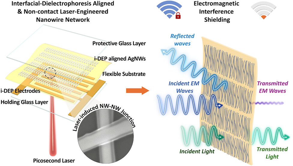
Instead of letting these wires spread randomly on a surface, they used a method called interfacial dielectrophoresis. In simple terms, they applied carefully shaped electric fields that gently pulled the nanowires into neat, well-aligned patterns on a flexible, transparent plastic film.
This approach allowed extraordinary control. The nanowires could bend, twist, and change direction without breaking alignment. To demonstrate this accuracy, the team even shaped the nanowires into readable letters on the film.
Importantly, the wires were aligned close to each other but not fused together. Tiny gaps remained between them, forming a network filled with nanoscale spaces. These gaps turned out to be essential.
When electromagnetic waves hit the film, the gaps behave like microscopic energy buffers, weakening the incoming signals before they can reach the protected electronics. This structure, described as a capacitively coupled nanowire network, dramatically boosts shielding performance without blocking light.
Strengthening the network with ultrafast laser pulses
 A diagram showing how EMI shielding is achieved using the nanowire film. Source: J. Zhang et al./ACS Nano 2025
In the second stage, the researchers exposed the aligned nanowires to extremely short bursts of laser light lasting just picoseconds. These laser pulses welded the nanowires together at their contact points, creating strong electrical pathways.
At the same time, the laser removed insulating surface layers left over from nanowire manufacturing. This single laser step delivered a rare double benefit. Electrical resistance dropped by 46 times, meaning electricity could flow much more easily.
Surprisingly, transparency also improved by up to 10 percent, because the laser cleaned the nanowire surfaces. This simultaneous improvement in conductivity and transparency had not been achieved before in metallic nanowire films.
When tested, the final material blocked more than 99.97 percent of electromagnetic radiation, achieving over 35 decibels of shielding effectiveness across frequencies from 2.2 to 6 gigahertz, which includes common Wi-Fi and 5G bands.
Despite this strong protection, the films remained 83 percent transparent and measured only 5.1 micrometres thick—thinner than a human hair.
“The electromagnetic interference shielding performance of the materials we created using this technique improves on the performance of non-aligned nanowires by more than a thousand times for the first time. That improvement could enable the creation of a wide range of future flexible and implantable devices,” Hadi Heidari, one of the study authors and a professor at the University of Glasgow, said.
The significance of good shielding
This work removes a major obstacle in the design of future electronics. Devices that must bend, stretch, or sit inside the human body can now be protected from electromagnetic noise without adding bulky metal layers.
“For flexible displays, wearable devices, and implantable medical technologies, this shielding capability, paired with a high degree of transparency, is crucial. It ensures high-purity signal transfer for real-time healthcare monitoring while blocking unwanted electromagnetic noise,” Zhang said.
Moreover, unlike traditional cleanroom fabrication, which is costly and size-limited, this approach can be scaled to large areas. The team has already produced films measuring 40 by 80 cm, suggesting that industrial production is realistic.
However, how the material will perform in the long term and within biological environments remains to be seen.
The study is published in the journal ACS Nano.

