

 Scientists at the University of St Andrews have unveiled a breakthrough that could change the future of holographic displays. Credit: Shutterstock
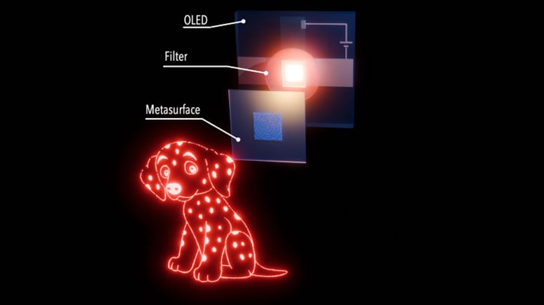
Researchers combined OLEDs with metasurfaces to project holograms. The method enables simpler, cheaper, and smaller displays.
New research from the University of St Andrews is advancing holographic technology, with potential applications in smart devices, communication, gaming, and entertainment. In a paper published in the journal Light, Science and Application, physicists from the School of Physics and Astronomy reported the creation of a new optoelectronic device that combines Holographic Metasurfaces (HMs) with Organic Light-Emitting Diodes (OLEDs).
Until now, holograms have typically been generated using lasers. The St Andrews team, however, demonstrated that pairing OLEDs with HMs provides a more compact and straightforward method. This approach is not only easier to implement but also less expensive, addressing one of the key challenges that has limited wider use of holographic technology.
 Credit: University of St Andrews
OLEDs are thin-film devices already common in mobile phone displays and some televisions, where they create colored pixels. Because they are flat and emit light across their surface, OLEDs are also promising for emerging fields such as optical wireless communication, biophotonics, and sensing. Their versatility and ability to integrate with other components make them well-suited for developing miniaturized, light-based systems.
A holographic metasurface is a thin, flat layer composed of nanoscale structures known as meta-atoms, each about a thousandth the width of a human hair. These structures are engineered to manipulate the behavior of light in precise ways. They can generate holograms and have potential uses in data storage, anti-counterfeiting technologies, optical displays, high-resolution microscopy, and sensing.
Generating holographic images
Researchers found that when each meta- atom is carefully shaped to control the properties of the beam of light that goes through it, it behaves as a pixel of the HM. When light goes through the HM, at each pixel, the properties of the light are slightly modified.
Thanks to these modifications, it is possible to create a pre-designed image on the other side, exploiting the principle of light interference, whereby light waves create complicated patterns when they interact with each other.
Expert perspectives and applications
Professor Ifor Samuel, from the School of Physics and Astronomy, said: “We are excited to demonstrate this new direction for OLEDs. By combining OLEDs with metasurfaces, we also open a new way of generating holograms and shaping light.”
Andrea Di Falco, professor in nano-photonics at the School of Physics and Astronomy, said: “Holographic metasurfaces are one of the most versatile material platforms to control light. With this work, we have removed one of the technological barriers that prevent the adoption of metamaterials in everyday applications. This breakthrough will enable a step change in the architecture of holographic displays for emerging applications, for example, in virtual and augmented reality.”
Professor Graham Turnbull, from the School of Physics and Astronomy, said: “OLED displays normally need thousands of pixels to create a simple picture. This new approach allows a complete image to be projected from a single OLED pixel!”
Until now, researchers could only make very simple shapes with OLEDs, which limited their usability in some applications. However, this breakthrough provides a path toward a miniaturised and highly integrated metasurface display.
Reference: “OLED illuminated metasurfaces for holographic image projection” by Junyi Gong, Mohammad Biabanifard, Kou Yoshida, Graham A. Turnbull, Andrea Di Falco and Ifor D. W. Samuel, 27 August 2025, Light: Science & Applications.
DOI: 10.1038/s41377-025-01912-z
Never miss a breakthrough: Join the SciTechDaily newsletter.