
In popular media, “AI” usually means large language models running in expensive, power-hungry data centers. For many applications, though, smaller models running on local hardware are a much better fit.
Autonomous vehicles need to respond in real-time, without data transmission delays. Medical and industrial applications often depend on sensitive data that cannot be shared with third parties. But even though edge AI applications can be faster and more secure, they have much more limited computing resources. They don’t have the luxury of terabyte memory footprints or effectively unlimited power.
Constraints that might be somewhat abstract for data centers impose hard limits on edge AI. In an invited paper and subsequent preprint from the 2025 IEEE International Memory Workshop, Onur Mutlu, professor of computer science at ETH, and his colleagues, noted that in typical mobile workloads, moving data to and from memory accounts for a staggering 62% of total energy consumption. Memory is the largest user of hardware real estate by a wide margin, yet memory delay is often the largest contributor to execution time.[1]
Device scaling, which for many years was the key to reduced power consumption, now makes the problem worse. Highly scaled DRAMs are less stable, Mutlu said, needing more frequent refresh cycles. Large memory arrays are harder to access, because bandwidth doesn’t grow as fast as the memory bank itself.
In-memory and near-memory computations offer possible solutions. Even commercial off-the-shelf DRAMs can perform primitive data copy, initialization, and bitwise logic operations, provided the software infrastructure supports them.
Hybrid solutions combine RRAMs, ferroelectrics
However, the problem of DRAM refresh power remains. In neural network models, both training and inference tasks make repeated use of a stored weight matrix. The two have contrasting requirements, though.
As Michele Martemucci and colleagues at CEA-Leti explained, training tasks involve many small updates to the weight matrix as it gradually converges to a stable value. These tasks demand memory with high write endurance and the ability to store precise values. Inference, in contrast, uses a stable, unchanging weight matrix, but might apply it to the input data many times. Inference tasks benefit from nonvolatile memory with high read endurance. In both cases, near-memory computation requires devices that are compatible with a standard CMOS logic process.[2]
RRAMs are simple devices that depend on a conductive filament formed in an oxide layer to achieve very high read endurance. With well-designed programming schemes, they can store analog values, reducing the size of the memory array. According to Martemucci, RRAMs are mature enough for commercial deployment in edge inference situations.
Unfortunately, RRAMs have relatively low write endurance. Over time, programming pulses can blur the resistance difference between stored values. Designers often train a model using conventional hardware, then load pre-calculated weights into an RRAM array. In many applications, though, the edge device needs to be able to “learn.” Either it needs to be trained for a user’s specific requirements, or the model needs to be modified to reflect changes in a real-world process.
Ferroelectric capacitors, meanwhile, support very fast switching with very high write endurance. They can easily tolerate the frequent write operations encountered in training tasks. However, while the stored value is nonvolatile, the read operation is destructive. These devices are not suitable for long-term storage of weight matrices, Martemucci said, or for inference tasks requiring frequent read operations.
Incorporating ferroelectric transistors into a CMOS process is complicated, requiring high-temperature processes and additional mask layers. Ferroelectric capacitors and tunnel junctions are much simpler, allowing several research groups to combine RRAM and ferroelectric structures. For example, in work presented at this year’s VLSI Technology Symposium, researchers at SK hynix demonstrated a hybrid ferroelectric tunnel junction (FTJ) with both resistive and ferroelectric switching.
In a conventional FTJ, the tunneling barrier between the top and bottom electrodes depends on the ferroelectric polarity. The SK hynix device sandwiched a ferroelectric hafnium zirconium oxide (HZO) layer between two electrodes, with a tantalum layer serving as an oxygen vacancy reservoir. Conductive filaments near the tantalum layer provided ohmic conduction in the top part of the device, reducing the effective thickness of the ferroelectric tunneling barrier. These devices achieved accurate analog multiply-accumulate operations, with efficiency as high as 224.4 trillion operations per watt (TOPS/W).[3]
In another hybrid approach, Martemucci’s group incorporated silicon-doped HfO2 capacitors with a titanium oxygen scavenging layer into a standard CMOS BEOL process. These devices initially behaved as ferroelectric capacitors, and some of them received a one-time “wake-up” pulse to stabilize the ferroelectric response. Meanwhile, another portion of the capacitor array underwent a one-time “forming” process, creating conductive filaments of oxygen vacancies. The titanium layer served as an oxygen vacancy reservoir, preventing dissolution of the filaments. The resulting memristor device could then be switched between high- and low-resistance states.
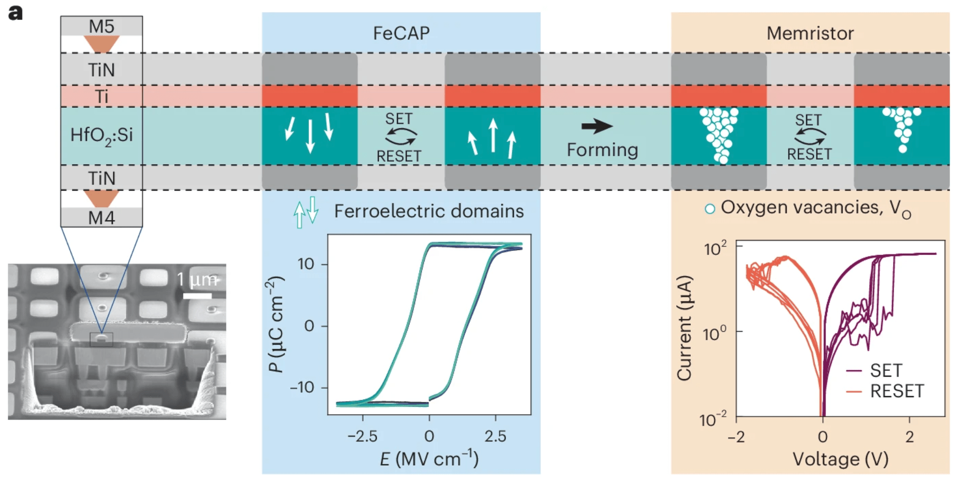
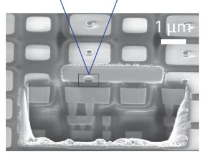
Fig. 1: The metal-ferroelectric-metal stack can be used as either an FeCAP or as a memristor. Source: CEA-Leti/Creative Commons License
The ferroelectric capacitors functioned as binary elements, storing high-precision weights for training calculations. The memristors stored analog weights with enough precision for inference tasks. During the training operation, the memristor array was updated after every hundredth input step, while the ferroelectric array was continuously updated. The total number of write operations to train this structure for a standard digit-recognition task was 17X smaller than the memristor endurance and 75X smaller than the ferroelectric capacitor endurance, while consuming 38X less energy than would have been needed to update the memristor array continuously.
More to AI than neural networks
While in-memory computation can make conventional neural network calculations more energy efficient, it facilitates alternative modeling approaches, too. For example, many computationally challenging problems can be modeled as Ising glasses, in which a group of connected nodes collectively evolves to a minimum energy state.[4] Real-world problems of this type might involve thousands or millions of connections.
Solving Ising glass problems is one of the more intriguing potential applications of quantum computing. More conventionally, at last year’s IEEE Electron Device Meeting, University of Texas researcher Tanvir Haider Pantha and his colleagues proposed building a 3D structure with FeFETs incorporated into the BEOL of a CMOS logic process. Each node, consisting of four cross-coupled FeFETs, can store a signed analog value, mapped to the Ising coupling matrix of the problem being solved. The output of each node is the input to its neighbors, setting up an oscillation through the entire network and ultimately reaching a stable, minimum energy configuration.[5]
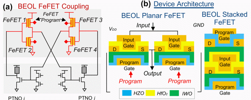
Fig. 2: Four cross-coupled dual-gated FeFETs form phase transition nano-oscillators. The proposed Ising glass model uses one of these structures per node. Source: IEDM
In-memory computation needs new frameworks
Conventional CPUs and GPUs are general-purpose devices. They can be applied to many different problems by simply changing their software. Near-memory and in-memory accelerators are currently inextricable from their intended tasks. An Ising glass solver, a point cloud network, and a network for image recognition will manipulate their data in different ways, requiring different hardware designs. According to Mutlu, the next step for in-memory computation will require software frameworks that can re-map memory access to meet the requirements of a particular problem. These frameworks, in turn, will require memory hardware that can manage itself, independent of an external memory controller.
References
Onur Mutlu, Ataberk Olgun, Ismail Emir Yuksel, “Memory-Centric Computing: Solving Computing’s Memory Problem,” https://arxiv.org/abs/2505.00458
Martemucci, M., Rummens, F., Malot, Y. et al., “A ferroelectric–memristor memory for both training and inference.” Nat Electron (2025). https://doi.org/10.1038/s41928-025-01454-7
W. -T. Koo et al., “224 Tops/W-Level Analog Computation in Memory Cell Using Hybrid Ferroelectric Tunnel Junction Having Enhanced on-State Conductance,” 2025 Symposium on VLSI Technology and Circuits (VLSI Technology and Circuits), Kyoto, Japan, 2025, pp. 1-3, doi: 10.23919/VLSITechnologyandCir65189.2025.11074955.
Andrew Lucas, “Ising formulations of many NP problems,” Front. Phys., 11 February 2014, Sec. Interdisciplinary Physics Volume 2 – 2014 | https://doi.org/10.3389/fphy.2014.00005
T. H. Pantha et al., “Towards 3D CMOS+X Ising Machines: Addressing the Connectivity Problem with Back-End-of-Line FeFETs,” 2024 IEEE International Electron Devices Meeting (IEDM), San Francisco, CA, USA, 2024, pp. 1-4, doi: 10.1109/IEDM50854.2024.10873406.