
Time-resolved measurement of plasmon wavepackets
Our quantum device consists of a 100 μm-long electron waveguide, fabricated by depositing electrostatic gate electrodes on a GaAs/AlGaAs heterostructure, as schematically drawn in Fig. 1a. The waveguide length can be adjusted using two segments, labelled w1 and w2. By applying a negative gate voltage to these surface gates (Vw1, Vw2), the underlying two-dimensional electron gas (2DEG) can be depleted, allowing for the formation of either a 50 μm waveguide (w2) or a 100 μm waveguide when both segments (w1 + w2) are combined. Electrons are injected into the 2DEG by applying a voltage pulse Vin(t), with variable duration, to the left Ohmic contact Oi, using an Arbitrary Waveform Generator (AWG, Keysight M8195A). They propagate in the form of a plasmon wavepacket through the quantum device. For detection, we utilise the right Ohmic contact, Oo, where the current is converted into voltage across a 10 kΩ resistor, then amplified and measured. The quantum point contacts (QPCs) at the entrances of the two waveguides, highlighted in red and blue, are used to locally control the number of transmitting electron conduction channels, while the QPC at the waveguide exit, highlighted in purple, is used to measure the speed of plasmon wavepackets via time-resolved measurements. Figure 1b illustrates the shape of the voltage pulses used in the measurement of this device. For our measurements, we applied voltage pulses with temporal widths varying from 52 ps to 500 ps. The displayed pulse shapes were recorded at the output of the AWG using a sampling oscilloscope at room temperature.
Fig. 1: Experimental setup and time-resolved measurement of plasmon wavepackets.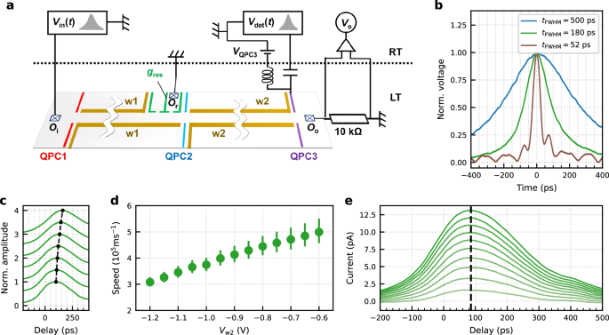
a Schematic of the device and the measurement setup. A 50 μm-long electron waveguide can be formed by polarising gates w2 and its length can be extended to 100 μm by additionally polarising gates w1, and \({g}_{{{{\rm{res}}}}}\). QPC1 and QPC2 are used to locally control the number of transmitting electron conduction channels for the 100 μm and 50 μm long waveguide, respectively. QPC3 is used for time-resolved measurements of plasmon wavepackets. A high bandwidth bias tee is connected to the upper QPC3 gate to be able to apply a fast voltage pulse, \({V}_{\det }(t)\) on top of the dc voltage, VQPC3. The reservoir gate \({g}_{{{{\rm{res}}}}}\) is used to connect the 100 μm-long electron waveguide to the Ohmic contact, Or. Plasmon wavepackets are excited by applying a voltage pulse, Vin(t), on the Ohmic contact, Oi. The output current at the Ohmic contact, Oo, is measured by the voltage, Vo across a cold 10 kΩ resistor. b Temporal shape of the voltage pulses generated by the AWG, with pulse widths defined by full width at half maximum (FWHM) ranging from 52 ps to 500 ps. c Time-resolved measurement of plasmon wavepackets excited by a 180 ps-long voltage pulse, for different wire widths in the 50 μm-long quantum wire. The vertical scale is normalised to one. Each curve is offset vertically for clarity. The voltage applied on the gates w2, Vw2 is changed from − 0.6 V at the bottom to − 1.2 V at the top by −0.1 V step. The peak positions are indicated with black points. d Speed of plasmon wavepackets excited by a 180 ps-long voltage pulse as a function of the gate voltage, Vw2. The speed is calculated from the length of the quantum wire and the delay time at the peak obtained as in (c). e Time-resolved measurements of plasmon wavepackets excited by a 180 ps-long voltage pulse with varying pulse amplitudes. The peak voltage at Oi is adjusted between 0.24 mV and 2.4 mV. The dashed line highlights the unchanged peak position despite varying pulse amplitudes. These characterisation measurements were conducted at 4 K.
Time-resolved measurements are performed using QPC3, which plays the role of an ultrafast on/off switch, thus enabling in-situ stroboscopic probing31. Initially, QPC3 is closed by applying a sufficiently large negative gate voltage to the DC port of the bias-tee, ensuring zero conductance across the waveguide. To probe the propagating wavepacket, QPC3 is briefly switched on by applying a 52 ps-long positive voltage pulse, \({V}_{\det }(t)\), to the upper gate of QPC3 through the RF port of the bias-tee. This pulse allows a small fraction of the plasmon wavepacket to pass through QPC3. By varying the time delay between the generation of the plasmon wavepacket triggered by a voltage pulse Vin(t) and the detection pulse \({V}_{\det }(t)\) at QPC3, we can reconstruct the temporal profile of the wavepacket in a time-resolved manner. To obtain an absolute value for the plasmon propagation speed, we carefully calibrate the length difference of the RF lines, using the known propagation speed of the two-dimensional plasmon (see Methods). To obtain a measurable current, we repeat the procedure at a repetition rate of 250 MHz. In addition, we modulate the injected pulse on Oi at 12 kHz and measure the output current at Oo with a lock-in technique to enhance the signal-to-noise ratio. The measured current at Oo, represents, in principle, the convolution of the plasmon wavepacket propagating through the electron waveguide with the time-dependent conductance across QPC3. The group velocity of the plasmon wavepacket, vp, is then calculated from the peak delay, tp, and the length of the quantum wire, \({L}_{{{{\rm{wire}}}}}\), using the relation \({v}_{{{{\rm{p}}}}}={L}_{{{{\rm{wire}}}}}/{t}_{{{{\rm{p}}}}}\). In the following, speed refers to the absolute value of the group velocity. According to the bosonisation formalism, plasmons have a linear dispersion relation and hence in principle their group velocity is equal to their phase velocity32.
As a control experiment, we perform time-resolved measurements of the plasmon wavepacket generated by a 180 ps-long voltage pulse in the 50 μm-long electron waveguide, varying the side gate voltage Vw2. This reduces the number of available electron conduction channels inside the waveguide, leading to a slowing down of the propagation, as demonstrated in ref. 31. Our experimental results (Fig. 1c, d) reproduce this behaviour, and the obtained propagation speeds are consistent with the previous study31. In the following measurements, we employ Vin with different temporal widths having a similar peak amplitude. The peak amplitude is slightly varied due to the bandwidth of the AWG, from 1.9 mV for the shortest (52 ps-long) voltage pulse to 2.6 mV for the longest (500 ps-long) voltage pulse. We carefully verified that for a given pulse width, the plasmon speed, or equivalently the peak position, is independent with respect to the peak amplitude. In Fig. 1e, we present representative data for a voltage pulse with a temporal width of 180 ps, demonstrating that the peak position remains constant regardless of the voltage pulse’s peak amplitude
Local control of transmitting electron channels
We now perform time-resolved measurements while controlling the number of transmitting electron conduction channels at QPC1 in the 100 μm-long electron waveguide. The voltage applied to the gates w1, w2 is set so that the waveguide accommodates more than 20 conduction channels. Figure 2a shows the results obtained with 52 ps-long voltage pulse. The pulse peak position, tp, stays fixed at 100 ps and does not shift when the number of the transmitting conduction channels through QPC1 is modified. In addition, the detected peak shape has a longer tail at larger time delays, showing additional peaks. In particular, the second peak appears around 220 ps, which is less than 3tp and hence it does not originate from the wavepacket reflected back and forth between QPC1 and QPC3. This result indicates that the plasmon wavepacket is being redistributed to the eigenstates formed by all the conduction channels in the waveguide after passing through QPC1, locally limiting the number of the transmitting conduction channels, which bears similarities to mode-matching in optics, when coupling multimode waveguide/cavity with different eigenmodes. This process is known as charge fractionalisation24. Our result shows the microscopic dynamics of this process.
Fig. 2: Local control of the number of transmitting electron conduction channels in 100 μm quantum wire.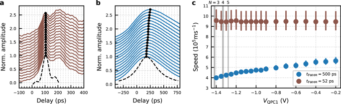
Time-resolved measurement of plasmon wavepackets excited by 52 ps-long voltage pulse (a) and 500 ps-long voltage pulse (b) for different voltages on the gates of QPC1. The amplitude is normalised to one. Each curve is offset vertically for clarity. The gate voltage VQPC1 was stepped from −0.2 V at the bottom to − 1.4 V at the top. The gate voltage Vw1,w2 was fixed to − 0.7 V. The peak position is indicated by the black circles. The shape of the voltage pulse used to excite the plasmon wavepacket is drawn by the black dashed line. c. Speed of the plasmon wavepackets calculated from the peak delay indicated by the black circles in (a, b). Here the number N on top of the grey shaded gate voltage indicates the number of transmitting electron channels across QPC1 at each voltage, which is determined by the observation of the quantised conductance.
On the other hand, when we perform the same measurement with 500 ps-long voltage pulses, a completely different result is obtained, as shown in Fig. 2b. Here, the peak position, tp, shifts to a larger delay when the number of the transmitting conduction channels is locally reduced at QPC1. The speed of the plasmon wavepackets as a function of VQPC1 calculated from the data in Fig. 2a, b is summarised in Fig. 2c. For the shorter pulse, the speed is constant as a function of VQPC1. This is caused by the redistribution of the wavepacket into the eigenstates of the waveguide right after QPC1. For the longer pulse, the speed is controlled by VQPC1 and hence by the number of the local transmitting conduction channels. This result implies that the charge fractionalisation process is suppressed for a longer plasmon wavepacket. Further to that, we note that the speed of the plasmon wavepackets generally decreases for those excited by longer pulses and should approach the Fermi velocity in the DC limit (see Supplementary Fig. 4 in details).
Fabry-Pérot cavity and electron-channel blockade
To interpret the behaviour observed in Fig. 2 we focus on the Fabry-Pérot (FP) cavity, which is formed between QPC1 at the entrance and QPC3 at the exit of the electron waveguide. For the time-resolved measurement, QPC3 is pinched off and is opened only for a short time, therefore forming one of the two end mirrors of the FP cavity. The second one is a partially transmitting end mirror to this FP cavity, formed by QPC1. As the FP cavity can be set to contain many conduction channels, when QPC1 is narrowed, electron conduction can only take place through a small number of transmitting channels. The channels that cannot transmit through the QPC are fully confined inside the FP cavity. The quantised energy levels of the FP cavity is the origin of the electron-channel blockade, as it allows for selecting the conduction channels contributing to the wavepacket transmission, when the matching conditions are met. Let us suppose that the electron waveguide contains N conduction channels and QPC1 is tuned to transmit exactly 1 conduction channel. In this case, (N − 1) conduction channels are confined inside the cavity. The resonant cavity condition is given by λm = 2LFP/m, where m is a positive integer corresponding to the mode number of the FP cavity. Similarly, the frequency components of the wavepacket that is transmitted through QPC1 should satisfy the resonant condition, fm = m ⋅ vp/(2LFP) = m ⋅ fFP, where vp is the speed of the plasmon wavepacket. On the other hand, the generated plasmon wavepacket is composed of many frequency harmonics, and its excitation spectrum has a bandwidth, Δf ~1/tFWHM, where tFWHM is the temporal width of full width at half maximum (FWHM) of the wavepacket (see Fig. 3b, c).
Fig. 3: Fabry-Pérot cavity and speed control with a local constriction.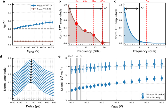
a The ratio between the frequency quantisation of the Fabry-Pérot cavity, fFP, and the bandwidth, Δf for the plasmon wavepackets. The dashed line indicates fFP/Δf = 1. fFP(=vp/2LFP) as a function of VQPC1 is calculated from vp in Fig. 2c. Δf( = 1/tFWHM) is calculated from tFWHM in Fig. 1b. Normalised amplitude of fast Fourier transform (FFT) of the voltage pulse in Fig. 1b for 52 ps-long voltage pulse (b) and 500 ps-long voltage pulse (c). The bandwidth value, Δf, is indicated by a black solid line. In addition, fFP at VQPC1 = −0.2 V and its multiples are indicated by the red dashed lines. d Time-resolved measurement of a plasmon wavepacket excited by 500 ps pulse for different gate voltages applied to QPC1 in the 100 μm-long electronic waveguide while it is connected to the Ohmic contact Or. The amplitude is normalised to one. Each curve is offset vertically for clarity. The gate voltage VQPC1 was stepped from −0.2 V (bottom) to −1.4 V (top). The peak position is indicated by the black dots. e Comparison of plasmon speed as a function of VQPC1 with and without the FP cavity for the wavepackets excited by 500 ps pulse. The data without the FP cavity (new data) and the data with the FP cavity (from Fig. 2c) is provided for direct comparison. Here, the number N on top of the grey shaded gate voltage indicates the number of transmitting electron channels across QPC1, which is determined by the observation of the quantised conductance.
When Δf is smaller than fFP, the frequency components necessary to construct a plasmon standing wave within the cavity are not available, and the (N−1) confined channels cannot contribute to the plasmon wavepacket transmission. As a result, charge fractionalisation to the (N−1) conduction channels is blocked. The plasmon is funnelled and transmitted only through the eigenstate of a single electron conduction channel. We call this phenomenon as electron-channel blockade for plasmon wavepackets. In the opposite limit Δf ≫ fFP, the Fabry-Pérot resonance condition is fulfilled, and as a result, a plasmon standing wave can be formed inside the FP cavity. For a non-interacting system, the plasmon can form a standing wave with a single conduction channel. A plasmon, however, is a collective excitation of interacting electrons. As it travels within the cavity, charge fractionalisation occurs and it will populate the eigenstates of the remaining N−1 conduction channels. In this situation the speed of plasmons cannot be controlled with the channel selection QPC, as the velocities within the cavity will be renormalised due to Coulomb interactions and an N-channel plasmon mode appears as a main component (for a detailed theory see the Supplementary Information in ref. 31).
Figure 3 a shows fFP/Δf calculated from the data in Fig. 2c for the plasmon wavepackets excited by a 52 ps and 500 ps-long voltage pulse. For the longer pulse fFP exceeds Δf for all VQPC1 values and hence electron-channel blockade occurs, enabling plasmon speed control with QPC1. Conversely, for the shorter pulse, fFP is a few times smaller than Δf. In this case, the plasmon speed remains constant with respect to VQPC1. Those observations are in line with our hypothesis discussed above. For fFP > Δf, which translates to Lp = vp ⋅ tFWHM > 2LFP, plasmon transport through the electron conduction channels confined inside the FP cavity is blocked and hence we can control the plasmon speed by locally changing the number of the transmitting conduction channels at QPCs. For Lp ≪ 2LFP charge fractionalisation occurs within the cavity and hence the plasmon eigenstate cannot be controlled by QPCs.
To confirm our hypothesis we intentionally break the FP cavity and demonstrate that, in this case, the QPC at the entrance of the waveguide is no longer effective to control the plasmon speed or its eigenstate. To do this, we completely depolarise the middle gate of \({g}_{{{{\rm{res}}}}}\), highlighted in green in Fig. 1a, to open the FP cavity towards the Ohmic contact Or. This connection to the Fermi sea reservoir breaks the FP cavity. We then perform time-resolved measurements as a function of VQPC1, for the 500 ps-long pulse, and compare the result with the configuration where the FP cavity is not broken (see Fig. 3d, e). When comparing the plasmon speed as a function of VQPC1, we observe that the plasmon travels significantly faster and shows smaller variation with VQPC1. In principle, we expect the plasmon speed to be entirely independent of VQPC1. However, this is not observed, as the opening to the reservoir accounts for less than 1 % of the total length of the FP cavity. As a result, the quality factor of the cavity is reduced, but the FP cavity is still influencing the plasmon speed. To further validate our observations, we confirm that in a three-terminal device (a quantum wire with two outputs), the local selection of the number of transmitting electron channels with a QPC does not affect the speed of plasmon wavepackets, as no FP cavity is involved (see Supplementary Fig. 6.)
The demonstrated electron channel blockade using an FP cavity originates from the narrower energy spectrum of plasmon wavepackets compared to the energy quantisation of the FP cavity. This mechanism is not affected by the energy fluctuation of the reservoirs at higher temperatures. Indeed, when we perform the same measurement as Fig. 2 at 4 K in a slightly different gate voltage configuration, we find the same tendency (see Supplementary Fig. 5). Here, the energy fluctuation of the reservoir is much larger than fFP of the FP cavity. This is in clear contrast to the Coulomb blockade of electron transport through a quantum dot, where the blockade is lifted at larger energy fluctuations of the reservoirs than the quantised energy of the quantum dot at high temperatures.
Suppression of charge fractionalisation in parallel waveguides
The conduction of electrons in two parallel, yet electrically isolated, electron waveguides can be considered independent. However, even though direct exchange of electrons is prohibited between the two parallel waveguides, electrons are coupled through Coulomb interactions. As a result, when a plasmon wavepacket is injected into one path of the two waveguides, charge fractionalisation occurs and a plasmon wavepacket is induced at the other waveguide23.
Here we demonstrate the suppression of the charge fractionalisation in such a parallel waveguides using the electron channel blockade demonstrated above. For this measurement, we use a device shown in Fig. 4a (see Method for details of the device). We form the two parallel electron waveguides by depleting the gates coloured in yellow. The two waveguides are electrically isolated by the middle gate along the waveguides and the upper gate at the entrance on the left, highlighted in purple. Plasmon wavepackets are injected by applying a 83 ps-long voltage pulse from an AWG (Keysight M8190A) on the left-most Ohmic contact, Oinj, with the peak amplitude of ~ 1.6 mV. They propagate through the lower electron waveguide and are collected in Ol. Here, plasmon wavepackets are expected to be induced at the upper electron waveguide23. To measure these induced wavepackets, we perform a time-resolved measurement using \({{{{\rm{QPC}}}}}_{\det }\) at the upper waveguide. For consistency, the probe pulse at \({{{{\rm{QPC}}}}}_{\det }\), is also 83 ps-long. In this device, we can form an FP cavity at the upper electron waveguide by using the gate, gFP, marked in red colour. When the FP cavity is not formed, the induced plasmon wavepacket is observed as expected (the blue curve in Fig. 4b). The shape of the induced wavepacket is similar to the derivative of the injected wavepacket, whose shape is characterised in a slightly different setup from Fig. 4a (see Supplementary Fig. 7 in details). The derivative-like shape can be understood as a current induced by the capacitive coupling with the charge of the injected wavepacket. On the other hand, by applying a large negative voltage on gFP to deplete the 2DEG underneath and by forming the FP cavity, there is no Coulomb-induced plasmon wavepacket as shown by the orange curve in Fig. 4b. When we estimate Lp and 2L in this situation, they are about 32 μm and 40 μm, respectively. While this does not strictly satisfy the condition for electron-channel blockade (Lp > 2L), the observed suppression of induced charge at Lp ~ 2L strongly suggests its effectiveness. Given the limitations in precisely quantifying this condition, we attribute this suppression to electron-channel blockade within the FP cavity formed on the upper quantum wire.
Fig. 4: Induced plasmon wavepacket in parallel electron waveguides.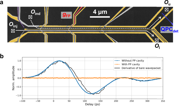
a SEM image of the device to investigate induced plasmon wavepackets. The gates coloured in yellow and purple are used to electrostatically form the circuit for the measurement. As a result, two parallel electron waveguides, which are electrically isolated, are defined. Time-resolved measurements of the induced plasmon wavepackets, injected at the Ohmic Oinj, are performed with the gate, \({{{{\rm{QPC}}}}}_{\det }\). A Fabry-Pérot (FP) cavity can be formed by creating a potential barrier with the gate, gFP, indicated in red. b Induced plasmon wavepacket without (blue curve) and with the FP cavity (orange curve). The amplitude is normalised with the maximum of the data without the FP cavity. The black solid curve is the derivative of the bare plasmon wavepacket measured in a slightly different setup (see Supplementary Fig. 7).
For a more quantitative understanding of the observed behaviour, numerical simulations would be useful. In a previous work, controlling the plasmon eigenstate by modifying the width of the whole waveguide was well understood with parameter-free numerical simulations31. However, direct application of the same numerical tool is not possible here due to the complex resonance behaviour of the FP cavity. The development of new numerical tools allowing for the simulation of the system with the FP cavity is desirable and will help us gain a deeper understanding of the system.
We have investigated the propagation of ultrashort plasmon wavepackets in a quantum nanoelectronic circuit while controlling the number of transmitting electron conduction channels at local constrictions. We found that an FP cavity formed by two potential barriers plays a critical role for the propagation of plasmon wavepackets. When the spatial length of the plasmon wavepacket, Lp( ≡ vp ⋅ tFWHM), is longer than double the length of the FP cavity, electron-channel blockade occurs, where plasmon eigenstate or speed can be controlled by changing the number of the transmitting conduction channels at local constrictions. Controlling the speed of ultrashort plasmonic excitations is attractive for quantum applications and the field of electron quantum optics. In particular, modifying the speed is equivalent to a phase delay and can be used for controlling the quantum state of a plasmon flying qubit3,21,33. With this method, a long one-dimensional system can be realised by placing a QPC at a distance L shorter than Lp/2 as shown in Fig. 5 and setting all the QPCs to allow transmission of only a single electron conduction channel. Since most of the electron waveguide can be kept wide, the stronger screening due to higher electron density makes plasmon wavepackets less vulnerable to potential fluctuations in the surrounding environment. Furthermore, electron-channel blockade can be used to suppress unwilling leakage of plasmon wavepackets to nearby circuits. This will contribute to high-fidelity operations of a plasmon quantum state. The capability to switch on or off the induced charge or more widely the propagation of a specific plasmon eigenstate may be of interest in applications for classical plasmonic circuits, like a plasmon transistor. We expect that the demonstrated electron-channel blockade will empower precise control of plasmon wavepackets in quasi-1D electron waveguides, significantly advancing the development of both quantum and high-frequency classical circuits based on plasmons.
Fig. 5: Schematic of the proposed device structure realising a clean and long one-dimensional system.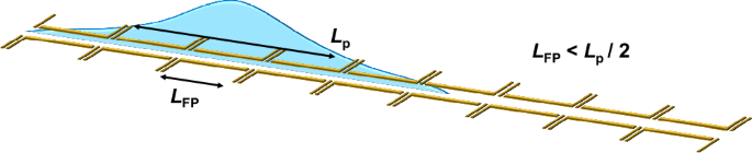
QPCs are placed at the distance, LFP, shorter than the half length of the plasmon wavepacket, Lp/2. When the number of transmitting channels is locally reduced to be one at each QPC, a clean and long one-dimensional system can be realised. Since the width of the quantum wires can be kept wide, the system is less vulnerable to the potential fluctuation of the surrounding environment due to the screening effect with electrons in many conduction channels.