
Intersubband transition and native-dielectric-doping
The intersubband transition energies in the WSe2 QWs can be approximated with an infinite square well potential with well width L = Nd, where N is number of layers and d is the monolayer thickness (Fig. 1a). The dispersion near the band edge at the Γ point can be obtained from
$${E}_{\Gamma }\left({k}_{z},{\boldsymbol{k}}\right)\approx -\frac{{\hslash }^{2}{k}_{z}^{2}}{2{m}_{v,z}}-\frac{{\hslash }^{2}{k}^{2}}{2{m}_{v,{xy}}}(1+\zeta {k}_{z}^{2})$$
(1)
where \({m}_{v,z}\) and \({m}_{v,{xy}}\) are the out-of-plane and in-plane effective masses, ζ is the nonlinearity parameter and \({k}_{z}\approx \frac{\pi n}{d(N+2v)}\)22. The intersubband transition energies can be expressed as
$$\left|{E}_{1}-{E}_{2}\right|=\frac{3{\pi }^{2}{\hslash }^{2}}{{2{m}_{v,z}d}^{2}{\left(N+2v\right)}^{2}}$$
(2)
and
$$\left|{E}_{2}-{E}_{3}\right|=\frac{5{\pi }^{2}{\hslash }^{2}}{{2{m}_{v,z}d}^{2}{\left(N+2v\right)}^{2}}$$
(3)
We compare the intersubband transition energies calculated with this modified infinite square well model with density function theory (DFT) and find a good agreement with experimental values21 (Fig. 1b). The intersubband transition energies in multilayer WSe2 can be tuned from 636 meV to 39 meV by control of the number of layers. To engineer optical access to the intersubband states in the mid-infrared energy range, typical of a QCL source, we specifically choose a platform of a five-layer (5 L) 2H-WSe2 homostructure to create a highly doped vdW multi-QW with accessible, partially occupied subbands. Figure 1c illustrates the fabrication process of WOx-doped WSe2 multilayers. In our method, the electronic band structure is, in essence, adjusted through the self-limiting oxidation of the top WSe2 layer. We subject a dry-transferred WSe2 flake to a UV-Ozone treatment, designed to convert the top layer into a TMO layer which has a high work function, while maintaining the atomic integrity of the underlying layers (see Methods and Supplementary Note 1). The significant work function difference between WOₓ and WSe2 induces a surface charge transfer32, promoting strong hole doping in the WSe2 layers. The hole density in these p-doped WSe2 multilayers is measured under ambient conditions using standard four-probe measurements (Supplementary Note 2). We find a hole density of p = 0.93 × 1013 cm−2 at VGS = 0 V, aligning with prior reports of doping in the 1013 cm−2 range29. By applying a back gate voltage, VGS, to the heavily doped Si substrate separated by the 300 nm silicon oxide layer, we can further increase this density to p = 1.11 × 1013 cm−2 at VGS = −25 V. The doping level achieved through the TMO layer process surpasses most electrostatic gating methods using solid dielectrics by an order of magnitude. Electrostatic approaches generally yield densities in the 1011 to 1012 cm−2 range33.
Fig. 1: Intersubband transition in WSe2 and WOx heterostructure.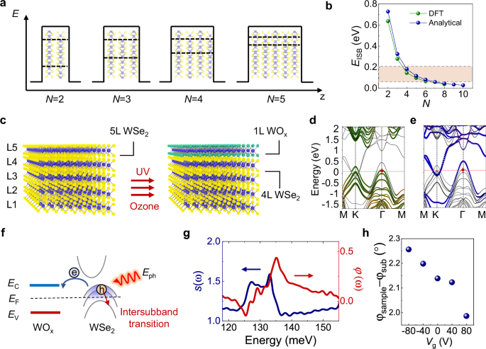
a Schematic illustration of subbands in the van der Waals (vdW) material quantum wells with different thickness defined by the number of layers N. Black dashed lines illustrate the subband energy positions. b Theoretical calculation of the intersubband transition energy of the first and second subband as a function of N for holes in the valence band using density function theory (DFT) (green circles) and modified infinite quantum well model, respectively. Red shaded area indicates the energy coverage of our mid-infrared laser. c Schematics of the doping process. Ultraviolet-ozone oxidation transforms the topmost layer of the 5L-WSe2 into transition metal oxides (TMOs) resulting in WOx/4L-WSe2. The oxidation process effectively doped the underneath WSe2 layers. DFT calculated band structure for WOx/4L-WSe2 heterostructure showing contribution from 4L-WSe2 in green (d) and top WOx layer in blue (e). Red dashed lines indicate the Fermi energy EF. Red solid arrows indicated the optical transition. f Illustration of charge transfer between WOx and WSe2 as the result of the work-function mismatch. EC is conduction band edge and EV is valence band edge;Excitation light with out-of-plane polarization can excite the charge carriers from the lower state to the upper excited state if excitation photon energy Eph is in resonant with the E23 intersubband transition energy. g Nano Fourier transform infrared spectrum of the WOx/4L-WSe2 near-field amplitude s(ω) and phase φ(ω). h Phase contrast between the sample and substrate as a function of gate voltage Vg.
We calculated the expected electronic band structure modification from the top WOx layer onto the WSe2 layers underneath, using density functional theory (DFT) incorporating spin-orbit coupling effects (Supplementary Note 2). Figure 1d, e presents the band structure of WOx/4L-WSe2 heterostructure calculated using this approach. These calculations elucidate the splitting of the highest valence band into multiple subbands at the Γ point in the Brillouin zone, corresponding to the interlayer coupling. Upon p-doping, free holes partially occupy these subbands from the subband base to the Fermi energy (EF), transitions can occur within the |k| ≤ kF range between a subband and a higher unoccupied subband. This is manifested as an absorption peak. To investigate the influence from the WOx layer, selenium atoms in the topmost layer were substituted with oxygen, and the ionic positions subsequently re-optimized. As depicted in Fig. 1d, e, this modification of the electronic states results in an altered band structure at the Γ point, displaying distinct subband splitting at mid-IR energies. Our calculation suggests that when the top layer (L5) is oxidized, the symmetry is broken and the top valence subband comes almost exclusively from the L5. The 2nd valence subband then comes mostly from L4 and L3 while the 3rd valence subband from L2. In order to maximize the coupling of light to intersubband transitions, it is desirable to populate holes in the second subbands in a few-layer WSe2, which requires carrier density more than ~1013 cm−2 and has been challenging to reach by electrostatic gating alone. In contrast, using the TMO layer we can easily generate the sufficient carrier density with EF positioned within the valence band. As illustrated in Fig. 1f, when the heterostructure is excited by photon with the out-of-plane polarization whose energy is resonant with the transition energy between the subbands, an intersubband transition between the second and third subbands can be observed.
Near-field imaging of the intersubband polaritons
An s-SNOM equipped with a broadband pulsed laser is utilized to carry out the nano-Fourier-transform infrared spectroscopy (nano-FTIR). The infrared excitation laser beam is focused on the metallized tip of the atomic force microscope (AFM), generating an enhanced optical field that interacts with the heterostructure sample beneath. With that configuration, we are able to characterize the intersubband transitions in WOx/4L-WSe2 at near-field with out-of-plane excitation polarization. The scattered light from the tip is collected, and the near-field amplitude and phase are recorded from the sample flake. This data is calibrated against a gold substrate to eliminate any instrumental responses. The near-field results provide insights into the sample’s complex permittivity, optical conductivity, and its absorption characteristics under the excitation energy Eph (Fig. 1g). Notably, while the dielectric response of WSe2 remains featureless from 120 meV to 160 meV34, WOx/4L-WSe2 heterostructure exhibits a distinct absorption peak, clearly indicative of the predicted intersubband transition. To avoid interference from SiO2 phonons, typically prominent around 140 meV, an Au/Si substrate without an SiO2 layer was utilized. We further explore the nano-FTIR result by fitting the data with modulated scattered field where tip-sample interaction and complex permittivity described as Lorentz model are taken into consideration (Supplementary Note 4). We then demonstrate intersubband absorption control by analyzing the phase contrast between the sample and the substrate φsample-φsub while changing the carrier density using a gate bias. The interferometric detection of the near-field optical response can decouple the amplitude and phase components from the scattered field as Escat ∝ Seiφ Ein, where S is the relative amplitude and φ is the phase shift35. Hence, the relative phase shift is a measurement of absorption at the near-field. As shown in Fig. 1h, we can clearly see that the absorption decreases when we inject electron into the sample to decrease the hole carrier density. (Note the electrostatic bias cannot tune the carrier density to the charge neutrality point due to the high doping level from the charge transfer of the WOx).
According to the nano-FTIR spectrum, the \({\varepsilon }_{{imag}}\) should exhibit strong resonant-like features along the out-of-plane crystal direction, implying the anisotropic dielectric permittivity should satisfy \({\varepsilon }_{{real},i}\times {\varepsilon }_{{real},j\ne i} < 0\), since the real and imaginary parts of the dielectric function are connected through the Kramers–Kroing relation36. Due to the different value of the effective masses and dielectric screening in the in-plane and out-of-plane directions, the highly doped WOx/4L-WSe2 heterostructure exhibits strong anisotropy in the frequency range (Fig. 2a). The heterostructure behaves like a dielectric in-plane, where \({\varepsilon }^{x,y} > 0\). For the out-of-plane direction, the heterostructure behaves like metal under the high carrier density conditions, showing a strong intersubband absorption with \({\varepsilon }^{z} < 0\) at the mid-IR frequency. We note that this phenomenon is fundamentally different from recently demonstrated bound carrier excitation in bulk WSe2 near the interband optical transition energy37. In the bulk WSe2 crystal, the subbands remain degenerate, and hyperbolic behavior emerges only under non-equilibrium conditions, in contrast to the ISPs studied here.
Fig. 2: Nano-imaging of intersubband transition and hyperbolic plasmon polariton in WOx/4L-WSe2.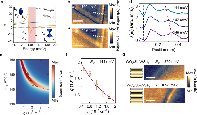
a Permittivity of the WSe2 (dashed lines) and with high carrier density under charge transfer (solid lines). Inset: the isofrequency surface modified from ellipse to a hyperboloid in the red-shaded region. Images of near-field scattering amplitude s(ω) for WOx/4L-WSe2 with excitation energy Eph = 144 meV (b) and Eph = 149 meV (c). The layer thickness is d ~ 4.5 nm. Scale bar: 500 nm. d Line traces of the interference pattern from the edge-reflected plasmon polariton taken from the near-field scattering amplitude image as illustrated in (b) and (c) (white dashed lines). Black dashed line marks the edge of the sample and red dashed line marks the peak position. e Dispersion of the intersubband polariton (ISP) in WOx/4L-WSe2. Color plot is calculated using the Fresnel reflection coefficients Im(rp). Yellow squares are experimental data. The error bars are determined from the fitting uncertainties of the fringe periodicities. f The extracted real part of momentum q as a function of carrier density n for WOx/4L-WSe2. The red solid line is the fit to the data using the relation \(q\approx 1/n\). The error bars are determined from the fitting uncertainties of the fringe periodicities. g Images of near-field scattering amplitude s(ω) for WOx/3L-WSe2 and WOx/5L-WSe2 with excitation energies Eph = 270 meV and Eph = 98 meV, respectively. Scale bar: 250 nm.
To effectively couple intersubband transitions to free-space photons and excite ISPs in the WSe2 quantum wells, we employed s-SNOM with both a continuous-wave QCL and a pulsed optical parametric oscillator laser to sweep across the transition energies. This configuration introduces an out-of-plane light component that drives the intersubband transitions within the heterostructure, thereby giving rise to ISPs. In order to reveal the ISP propagation in the heterostructure, we now investigate the polariton dispersive dynamics interferometrically using the real-space near-field nano-imaging technique. Figure 2b, c presents data collected at different excitation energies, Eph = 144 meV and Eph = 149 meV, respectively. Oscillations of the near-field amplitude s(ω) are observable at the flake edge. These fringes arise from the interference between the tip-launched polariton and the propagated polariton reflected at the sample edge. By examining the cross-sectional profile perpendicular to the sample edge, we can extract the periodicity of the bright-dark fringes, which corresponds to half of the polariton wavelength (λISP/2). As the excitation energy increases from 144 meV to 149 meV, the polariton wavelength increases from 317 ± 10 nm to 453 ± 12 nm (Fig. 2d). The propagation length of the ISP is fitted to be 0.8 μm (Supplementary Note 5). The lifetime of the ISP is calculated as \({\tau }_{{\rm{ISP}}}=\frac{L}{{v}_{g}}=0.4{ps}\) (Supplementary Note 10). Using the same method, we systematically extract the polariton wavelengths at various tuned excitation energies from the nano-imaging data. The confinement factor \({\lambda }_{0}/{\lambda }_{{ISP}}\) reaches up to 27, comparable to that of plasmon polaritons in graphene and phonon polaritons in h-BN, while still smaller than the acoustic plasmon in graphene38. We visualize the dispersion relations with a false color mapping of the imaginary part of the reflection coefficients Im (rp), representing the photonic density of states as a function of wave vector \(q=2\pi /{\lambda }_{{ISP}}\) (Fig. 2e and Supplementary Note 6). This inverse relationship between energy and momentum confirms the Type I hyperbolic polariton dispersion, where \({\varepsilon }^{z} < 0\) and \({\varepsilon }^{x,y} > 0\).
As noted, in addition to the charge transfer process via TMO layer, the carrier density can be further tuned. We demonstrate the electrical control of the polaritons by systematically tuning of the intersubband transitions in the valence band via back-gating. Since the charge transfer method between the TMO layer and WSe2 drives a much higher carrier density than that possible via tuning by electrostatic gating, we can vary the carrier density modestly in the p-type doping regime. Figure 2f shows the ISP momentum q as a function of the back-gate voltage Vg at a representative energy Eph = 144 meV. The magnitude of q is approximately proportional to n−1, where higher hole density leads to increased negative permittivity39. The evolution of q with Vg further confirms the hole doping in the WOₓ/4L-WSe2 structure and the observed negative dispersion relation (Supplementary Note 8). Such active tunability is generally absent in the natural hyperbolic materials such as h-BN40 and MoO341. The intersubband transition energy can be controlled with the thickness of the vdW layers. We also demonstrated the nano-imaging of the ISP in both WOx/3L-WSe2 and WOx/5L-WSe2 heterostructure at excitation wavelength Eph = 270 meV and Eph = 98 meV, respectively (Fig. 2g). This finding aligns well with the theoretical calculation shown in Fig. 1b.
Measurement of the hyperbolic propagation
We explore the presence of hyperbolic ISP by positioning the WOx/4L-WSe2 heterostructure on the 50 nm Au disk (Fig. 3b). The conical-shaped rays launched by the edge of the Au disk will reach the top surface of the heterostructure forming bright rings separated by the edge (Fig. 3a). The distance between the bright ring and the electrostatic edge, denoted as ΔR, is modulated by the isotropic components of the dielectric tensor, with the relationship \(\Delta R/d=\left|\tan \theta \right|=i\sqrt{{\varepsilon }_{{xy}}}/\sqrt{{\varepsilon }_{z}}\), where d represents the heterostructure’s thickness, and θ is the angle from the surface normal42,43. Directional propagation of the hyperbolic ISP along the resonance cone is observed at Eph = 145 meV (Fig. 3c). The line-profiles taken from the s-SNOM amplitude image reveal that the radial distance ΔR is significantly smaller than that observed in bulk hyperbolic materials, due to the thickness of the heterostructure as thin as d ~ 4.5 nm (Fig. 3d). We further verify the hot-ring feature for different layer number samples by transferring the heterostructure with different thickness onto the same Au disk. When the excitation energy matches the E23 transition energy of the WOx/6L-WSe2 at Eph = 114 meV, we can see only the bottom half lights up (Fig. 3e). When we increase the excitation energy to Eph = 146 meV, the upper half lights up as the intersubband transition energy increases with the fewer layer numbers (Fig. 3f). The layer-dependent hyperbolicity highlights ISPs as a promising addition to the family of hyperbolic polaritons, complementing other recently demonstrated phenomena such as topological transitions44, negative refraction45,46, and low-loss propagation47.
Fig. 3: Hyperbolic ISP revealed by nano-imaging on Au nanodisk.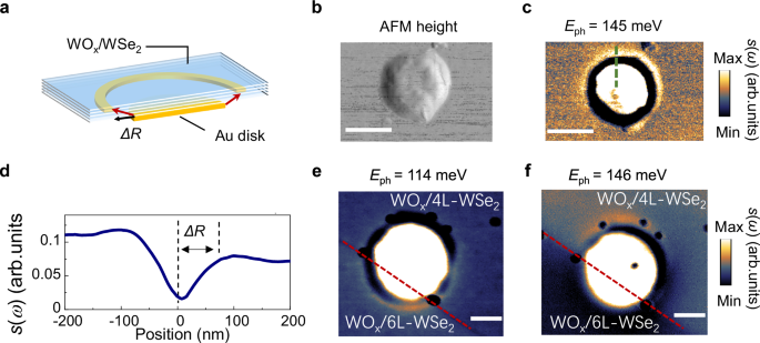
a Schematic of hyperbolic polaritons launched at the edge of the Au nanodisk, which travel along conical trajectories and form a bright ring. The distance between the ring and the edge of the Au nanodisk is ∆R. Topography (b) and near-field scattering amplitude s(ω) image of WOx/4L-WSe2 plasmonic cavity with diameter D = 300 nm and excitation energy Eph = 145 meV (c). Scale bar: 300 nm. d Line profile of the measured near-field amplitude taken at the dashed line in (c). Near-field scattering amplitude s(ω) image of sample on the Au nanodisk that is partially covered by WOx/4L-WSe2 and WOx/6L-WSe2 simultaneously and excited with Eph = 114 meV (e) and Eph = 146 meV (f), respectively. Red dashed lines indicate the boundary. Scale bar: 150 nm.
Intersubband polaritons in nanoresonators
We further manipulate the hyperbolic ISP by fabricate the WOₓ/4L-WSe2 heterostructure into nanoresonators where the polariton modes are confined by the circular boundaries. Figure 4a illustrates the schematic of an s-SNOM measurement conducted on focus ion beam (FIB) patterned WOₓ/4L-WSe2 nanoresonators with an underlying gold mirror. By eliminating the need for a polymer mask in the etching process, direct FIB fabrication keeps the heterostructure surface uncontaminated, minimizing the risk of residue deposition or chemical interaction commonly associated with mask-based techniques, thereby preserving the material’s intrinsic properties and optimizing the quality of subsequent device performance. Additionally, a gold mirror is deposited on the substrate to minimize radiative decay into the silicon substrate, thereby resulting in lower loss and longer lifetime (Supplementary Notes 9 and 10). To explore the relation between the resonant energy and the diameters of the nanoresonators, we patterned disk nanoresonators with diameters ranging from 100 nm to 800 nm. The propagation of the ISP in the nanoresonators can be described by the wave equation \({\rho (i\omega )}^{2}={\nabla }^{2}\rho {v}_{p}^{2}(\omega )\), where ρ denotes the integrated two-dimensional charge density and vp is the group velocity48. For a disk-shaped resonator, the solution of ρ can be expressed in terms of Bessel functions, with the eigenvalues ksn determined by the disk diameter. Consequently, because the ISP can resonate only with resonators of specific sizes at a given excitation photon energy, tuning the Eph enables the systematic mapping of the relationship between disk diameter and the ISP resonant modes (Fig. 4b).
Fig. 4: Intersubband polariton confined in WOx/4L-WSe2/Au nanoresonators.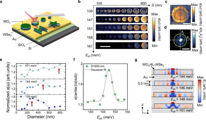
a Schematics of WOx/4L-WSe2/Au nanoresonators fabricated by focused ion beam on gold substrate. b Near-field scattering amplitude s(ω) images of an array of WOx/4L-WSe2/Au nanoresonators with different diameters (100 nm to 800 nm) and different shapes. The images are measured at a series of excitation energies from 139 meV to 161 meV. Scale bar: 1 μm. c Near-field scattering amplitude s(ω) image of WOx/4L-WSe2/Au nanoresonator with diameter D = 600 nm. The excitation energy is Eph = 146 meV. Scale bar: 250 nm. d The corresponding Fourier transform image of (c). kx and ky are wavevectors in x and y direction. Scale bar: 40 k0, where k0 is the momentum of light in free space. e Normalized near-field scattering amplitude as a function of diameters of the resonators with excitation energy at Eph = 151 meV (top panel), Eph = 144 meV (middle panel) and Eph = 139 meV (bottom panel). Red arrows help to identify the peak value of s(ω). f Normalized amplitude as a function of excitation energy for the WOx/4L-WSe2/Au nanoresonator with diameter D = 600 nm (green circles). Gray solid line is the Gaussian fitting. g Finite-difference time-domain simulation of the out-of-plane field Ez in WOx/4L-WSe2/Au nanoresonator with different excitation energies of Eph = 144 meV, Eph = 146 meV, Eph = 148 meV and Eph = 151 meV, respectively. The diameter of the nanoresonator is D = 600 nm.
To quantitatively study the confined mode in the resonators, we analyzed each disk resonator at different excitation energies. The near-field amplitude image of a representative nanoresonator with a diameter of D = 500 nm is shown in Fig. 4c, where a standing-wave pattern with multiple fringes emerges49,50. Figure 4d presents the Fourier transform |s(kx, ky)| of the near-field amplitude image from Fig. 4c, revealing the iso-frequency contours for the ISP at 146 meV. The in-plane permittivity of the WOₓ/4L-WSe2 heterostructure is isotropic. We then extract the near-field amplitude response from the standing wave in the resonator at different excitation energies (Fig. 4e). The signal was normalized to the background at the surrounding gold surface to compensate for variations in the laser power and optical alignment in each measurement. At Eph = 139 meV, the near-field amplitude shows a peak D = 300 nm. The size of the resonator imposes a constraint on the ISP wavelength confined in the resonator. With increasing Eph, disk diameter exhibiting a stronger scattered near-field response also increases due to the longer polariton wavelength, aligning with the hyperbolic dispersion relation observed in the unpatterned heterostructures. We then investigate the field concentration and the resonance behavior of the confined ISP by analyzing a resonator with D = 600 nm under various excitation energies. Figure 4f shows the near-field optical response as a function of the excitation energy. The signal is normalized to the substrate background to eliminate the influence from the power stability and detection efficiency. We fit the peak with Gaussian function with center energy at 147 meV and FWHM = 3.2 ± 0.3 meV. The quality factor is then calculated as Q = ω/FWHM = 45.9, where ω is the resonant frequency48,51.
We finally conducted a numerical simulation for the resonator with same diameter of D = 600 nm to further explore the polaritons propagation in WOₓ/4L-WSe2 nanoresonators. The z-component electric field distribution, mapped at various excitation energies in Fig. 4f, shows that as the Eph increases from 144 meV to 148 meV, the distance between the bright maxima widens, following the negative dispersion relation. At an Eph = 151 meV, the polariton wavelength λISP = 478 nm exceeds the nanoresonator’s radius, precluding effective ISP mode confinement. Our FDTD simulations show that the highly confined modes have an effective mode volume V of \(2\times {10}^{-6}/{\lambda }_{0}^{3}\), respective to the free space photon wavelength λ0, which quantifies the strong spatial confinement of light in the disk nanoresonators52. These observations highlight that the structural refinement of nanoresonators via FIB patterning facilitates enhanced control over polariton modes, resulting in a higher quality factor and improved mode confinement. Importantly, there remains potential to further optimize the cavity design to achieve even greater polariton confinement with a significantly reduced mode volume53.