
Key Takeaways
Scaling to 2nm and below continues due to power improvements per watt, but progress is much more challenging and costly.
Solutions to problems often create other problems due to less margin for tradeoffs, often requiring larger interposers, more chiplets, and more complex packages.
New levels of precision are required throughout the design-through-manufacturing flow, resulting in shifts to some technologies that have been sitting on the sidelines for years.
Designing, developing, and manufacturing chips at 2nm and below requires a whole new set of business and technology tradeoffs that are dramatically more impactful at every turn, from architectural inception to manufacturing yield.
The primary goal of shrinking features at these dimensions is orders of magnitude performance improvements per watt, but it’s not as straightforward as packing more transistors onto a piece of silicon. At these dimensions, several atoms of variation, or a nanoscale void or burr in a signal path, can impact performance. Wires and metal layers are getting so thin that any anomaly can cause unplanned-for thermal gradients and thermal migration, reducing reliability and shortening the lifespan of a device. And materials such as resists and bonds need to be so pure that contamination must be measured in parts per quadrillion.
Complexity is exploding on every level, and it can have ripple effects in unexpected places. Multi-die assemblies can include tens or hundreds of billions of transistors, multiple different kinds of memories, and multi-level/multi-die routing and power delivery schemes. Managing all of this locally and globally requires multiple areas of expertise that cut across traditional silos, and multiple iterations over nearly everything.
“There is a set of patterning and materials complexity in metal-0 through metal-3 that is extremely high,” said David Fried, corporate vice president at Lam Research. “I’m a transistor guy, so I would always say that the higher orders of complexity are in the transistor. If you look at 2nm logic, we’re talking about gate-all-around nanosheet devices. The three-dimensional complexity of those transistors is extraordinary. The transition from finFET to gate-all-around nanowire is an order of magnitude more complex than the previous transition. From a structural complexity perspective, there are many more materials in play in the front end of the technology. Once you get to metal-0 through metal-3, those layers have a smaller material set. You’re typically at slightly tighter patterning, slightly smaller features, but a much smaller materials set and fewer key performance indicators like resistance, capacitance, some structural integrity parameters, some reliability. But when it comes to managing transistor performance, you have many different performance metrics at lower levels.”
From an economics standpoint, nearly all designs at the leading edge are vendor- or workload-specific. Companies with deep enough pockets to pay for these very expensive advanced-node chips want them customized for specific data types and operating conditions, and they want to be able to leverage that customization across multiple generations of derivative chips. At the same time, foundries need to be able to extend their investments beyond just one customer. The way to satisfy both is by using common metal layers lower in the stack, often developed with the help of some very expensive tools and equipment, while adding more customization further up the metal stack.
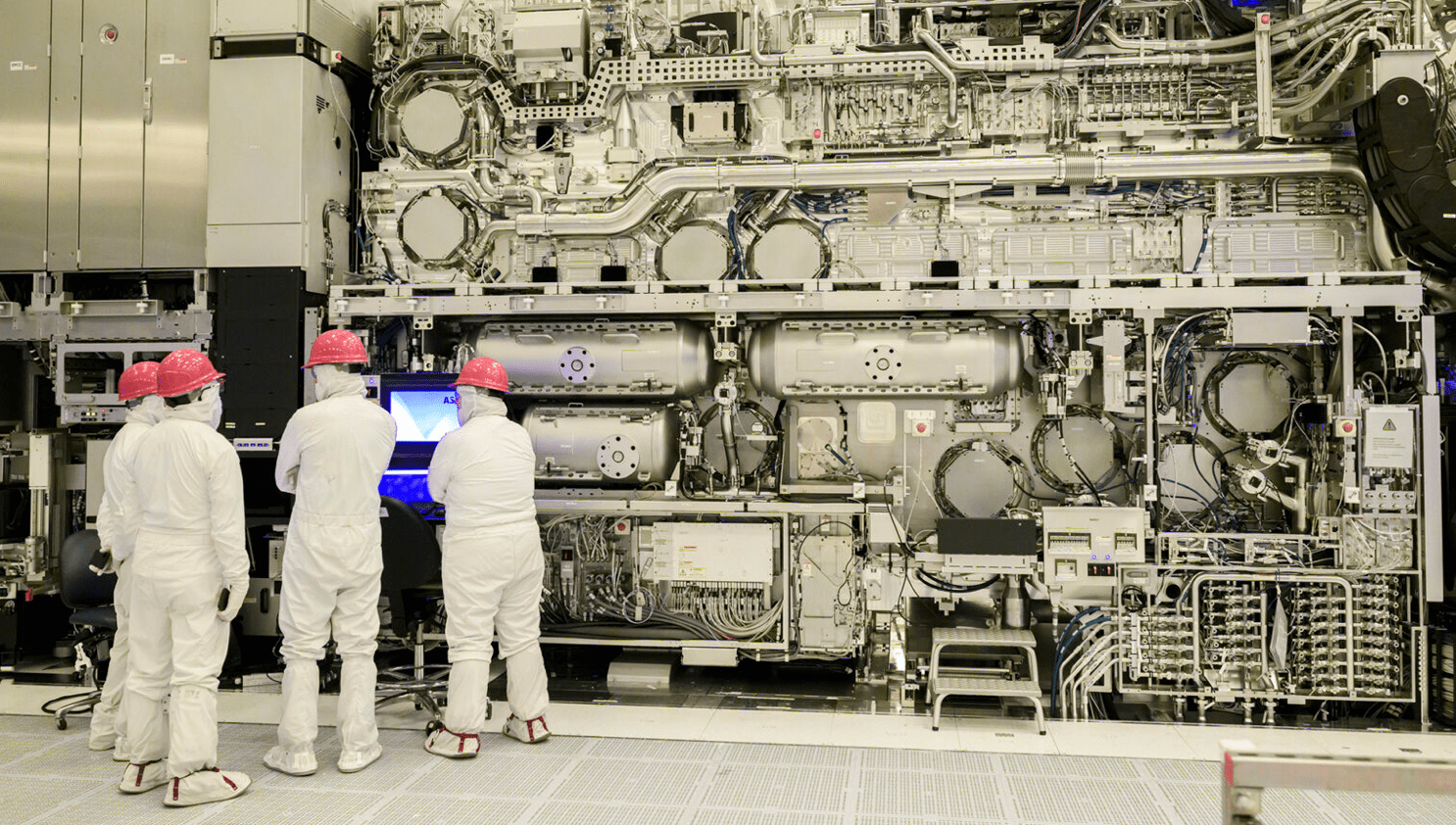
Fig. 1: Intel’s 165-ton high-NA EUV scanner, priced at $350+ million. Image source: Intel Foundry
“It’s very useful when the foundry can standardize a few layers with basically the same process,” said Kostas Adam, vice president of engineering at Synopsys. “This includes metal-0 to metal-3, and usually also the middle metallization layers, metal 4 and 5, although it can keep going up to 12. But that doesn’t change the fact that each of these layers holds a different routing configuration. Each of these layers requires its own computation to produce the mask and print that specific layer. But then the foundries offer variants. So it’s not like there is a 2-nanometer process and that’s it for everybody. There’s a certain level of customization that is possible. For example, a high-profile customer may need a few more layers on their metallization process to give it higher performance, and that makes for more interesting management of the complexity on the fab side.”
That only adds to the challenges. “The more stuff you throw together, the more you need co-optimizations of multiple effects, all at the same time,” Adam said. “So the computation is rising, and the complexity of dealing with all these kinds of things together becomes more interesting.”
Those choices also add to the cost, which can easily top $100 million from design to working silicon. And while that may seem like an enormous up-front investment, the benefits of lower power and improved performance (less cooling, lower energy costs) can be many times as much for AI data centers.
“For some of our customers, we have three bottom die, and then we stack an Intel 18A on top of this,” said Ben Sell, vice president and general manager of logic technology development at Intel. “Right now we’re using what we call Foveros, which is a microbump at a certain pitch. It can be 35 or 25 microns, and you stack these dies bump-to-bump to get a higher density of signals for chip-to-chip communication. You really want to scale the pitch of these connections, and that’s where hybrid bonding comes in. If you look at the next set of products we’re releasing, we’re changing to a 9-micron hybrid bonding pitch so you get much denser connections from chip-to-chip. This is one way that really helps us to scale the chip connection, going from bumps to hybrid bonding.”
Nearly all of these leading-edge chips are heterogeneous. While some of the logic uses a 2nm or 18 angstrom process, most of these designs are packaged with dies developed at older technologies, as well. Mixing manufacturing processes is nothing new, but the volume and potential impact of these combinations is increasingly challenging. Large systems companies such as Google, Tesla, Microsoft, and Meta are constantly pushing for higher performance, which requires more area than a single reticle can provide. The solution, at least so far, has been to divide different functions into chiplets and connect them using an interposer, which allows for much higher logic density per system than a single reticle-sized SoC can provide. But this can easily evolve from a difficult challenge to an unworkable one as the number of chiplets increases.
“Monolithic scaling alone is no longer sufficient,” said Evelyn Landman, CTO at proteanTecs. “Multi-die architectures will continue to expand because they scale performance, enable heterogeneity, and improve economics. This is increasingly visible in advanced compute roadmaps of the industry leaders. The challenge shifts from building a large die to ensuring that many dies behave as a coherent system over time. Chiplets trade one class of risk for another, including interconnect effects, package-induced variation, and debug complexity, yield, and operational economics. These risks must be actively managed rather than assumed away simply because these issues didn’t exist previously.”
Managing the signal traffic between chiplets developed at different nodes adds yet other challenges, because the I/O speeds and data movement at older nodes are typically slower. This requires more granular control and prioritization of data as it moves between processing elements and memory.
“If you want a much larger system, maybe 100 x 100 millimeters, either you build a really large interposer or you build small bridges that just connect dies you place next to each other,” Sell said. “It’s a lot more economical to build bridges for tens of dies than to have a giant interposer that you bond everything on top of.”
Tougher tradeoffs
Shrinking dimensions affects every process in a fab, and every piece of equipment tied to those processes.
“Before you get to using interposers and things like that to connect chips at different technology nodes, particularly for the more advanced leading edge, you do a lot of things with wafer thinning, through-silicon vias, and backside power delivery where you thin the wafer down as far as 10 microns thick,” said Synopsys’ Adam. “They describe this as a potato chip because the stress effects cause the wafer to deform like one. And unless you take this into account carefully in manufacturing, it can cause very serious misalignment issues when you try to stack one thin die on top of another. That problem is very prevalent on high-bandwidth memories that have 12 to 16 dies stacked one on top of another.”
Every decision made at the leading edge has repercussions, some upstream, more downstream. “We need to make sure 2nm technology is going to work well with the packaging,” said Rozalia Beica, field CTO for packaging technologies at Rapidus Design Solutions. “We are developing the packaging technologies. At the same time, we are building the ecosystem. And now, with EDA, we are getting all the IPs that we need. We have the tools for the rapid assisted design services that we will provide as an option to the customers. Bringing all these together is going to be very difficult. Manufacturing is planned for 2027 for the silicon technology, and then packaging in 2028. There are still a few years for us to prepare and address all the different challenges, and to learn about them, too.”
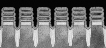
Fig. 2: Rapidus licensed IBM’s 2nm nanosheet technology, which leverages a multi-Vt approach to reduce the energy needed to perform complex computations. Source: IBM Research
The biggest advantage of scaling to the most advanced nodes is power reduction/mm2. Scaling just to pack in more transistors — which prior to the finFET era used to be the standard approach for improving performance — has resulted in limited performance improvements for the past five process nodes. Results vary by foundry, but those improvements have been no higher than 20% per node (and sometimes as little as single digits), and often were traded off entirely for a reduced power budget. That, in turn, led to a proliferation of 2.5D architectures inside of AI data centers, comprised of general-purpose processors and highly specific accelerators, connected with a large silicon interposer.
CPUs, GPUs, DSPs, MCUs, and FPGAs fall into the general-purpose category, while NPUs and TPUs are used for specific data types. There are some new hybrids on the market, as well, such as Arm’s new AGI CPU, and some of the neuromorphic processors. But to achieve orders of magnitude improvements in performance, some combination of processor types is needed, whether that is integrated on a single die, or connected together inside package, on a board, or in a rack. And in all cases, that requires significant amounts of cooling and monitoring of devices to ensure clear data paths between processors and memories.
In addition, scaling beyond 3nm has increased gate leakage to the point where finFETs are becoming a significant current leakage problem once again. That, in turn, increases the thermal density, and exacerbates the challenge of thermal dissipation. The fix, at least for now, is the gate-all-around FET (aka nanosheets), but chipmakers are working on complementary FET processes, which are expected sometime within the next few angstrom nodes.
Big picture problem solving
What becomes clear at 2nm and beyond is that nearly all challenges are connected. Solving one in isolation likely results in increasingly challenging problems somewhere else.
“Margin becomes one of the most contested resources at 2nm and 18A,” said proteanTecs’ Landman. “There needs to be enough margin for process variation, thermal and environmental effects, workload stress, latent defects, and aging. Aggregating all of these into a single worst-case guard band is no longer viable. Static guard-band sacrifices performance and power and still fails to protect against real-world field conditions. The only sustainable approach is to measure the guard-bands directly, by monitoring timing margin in real-time, at high coverage, under real workloads, and managing it continuously over the product lifetime. The idea is to monitor guard-bands as first-order effects by measuring timing margin, not by proxy.”
Combined with faster interconnects, optimization for different types of data, algorithmic quantization, and co-design of software and hardware, significant improvements in performance are being achieved. But how they achieve that performance improvement can vary greatly.
“There are many different options for how to integrate different subsystems,” said Lam’s Fried. “If you want to integrate high-speed memory, your highest priority will be performance and bandwidth. If you want to integrate your largest logic with an optical interconnect, then you might be governed more by size and thermal constraints. It comes down to understanding constraints for the full level of system integration. There will always be multiple options for this. 3D packaging and heterogeneous opened up this whole new access for optimization. What that means is every system is going to find a set of optimized solutions for how it comes together. That’s the coolest part of this. You now have a whole new set of axes for optimization, but variability is going to be a concern in every piece of this.”
Put simply, each new node, and each new multi-die architecture, involves more interactions with less engineering wiggle room. But that isn’t the end of the road for scaling. Performance and power could improve another order of magnitude or more if true 3D-IC designs are successfully deployed. This is largely due to the fact that distances the signals need to travel vertically between logic and memory will be significantly shorter, with less resistance, than on a relatively thick silicon interposer. And with hybrid bonding, those signals can be routed more quickly.
Numerous industry sources confirm that full 3D-ICs are in development, though none are in production yet. It’s still not clear if any of them will be sold commercially, or how much information will be publicly available if they are successful. Most of these designs will be customized for different data centers, and how they work (or where they may stumble) is highly competitive information. What’s clear, though, is the challenges there are both significant and additive — optimal floor planning, thinner dies and substrates, handling issues, warpage, inspection and test accessibility, signal integrity and traffic control, lattice mismatch management, electromigration, accelerated aging, and thermal dissipation.
And that’s just for the known constraints. These chips are being developed at the leading edge of physics, where surprises are not uncommon. In some cases, those surprises have been positive.
“We have actually not seen the gate oxide quality be impacted by mechanical stress,” said Intel’s Sell. “We have a lot of mechanical stress to improve the drive current, and in many cases the mechanical stress helps you, and especially for the pMOS device, it helps you for aging. It’s just the way it aligns the band gap of the device. We see that higher stress for the rise is actually better for aging.”
In other cases, not so positive. Variation is a tougher challenge at each new node, and it needs to be addressed progressively earlier in the manufacturing flow, and in more process steps, as dimensions shrink and tolerances tighten.
“You have to get the first layer right,” said John Holt, manager of Fab Applications Solutions at PDF Solutions. “There is a margin of error that just gives enough energy for an atom to diffuse to the interface, and enough to diffuse through one additional layer. The foundries can very tightly control the deposition. But there is also natural variability, and not just on that step. So if you’re looking at a CD (critical dimension), you have to look at the conditions of the wafer coming in prior to patterning — the thickness, the reflectivity — and then you coat the wafer and develop it. That takes into account all the environmental variables to put a photoresist-sensitive layer on there so you can pattern it. We found these lens optics are really sensitive to any temperature changes, so you’re looking at the optics, too. And then you have to look at the next step, which is the etch. How does it etch across very sparse geometries? And these are just two steps in the manufacturing process. Now you have to implant the source drain, so now you have another source of variability. If you don’t look at this holistically, you’re not going to be successful.”
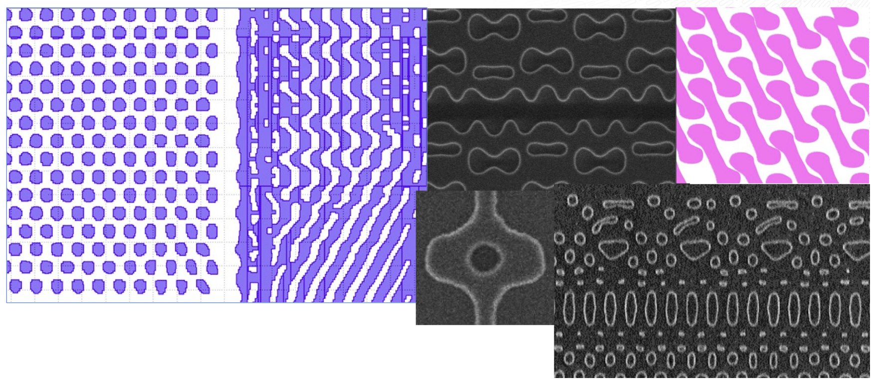
For years, the chip industry has been developing a variety of technologies and processes that might someday be needed, but which often are sidelined until absolutely necessary. This includes high-NA EUV, which enables sub-2nm transistors to be printed on silicon, as well as advancements in multi-beam e-beam technology, which ensure that what gets printed on a photomask matches what’s supposed to be printed on the silicon. Aki Fujimura, CEO of D2S, said in a recent presentation that as these chips get larger in area, the accuracy of OPC masks decreases. By replacing polygons with curvilinear shapes, the accuracy of what gets printed increases dramatically, which in turn improves yield for the angstrom age.
Fig. 3: Curvilinear patterning on a photomask. Source: Micron/D2S
The future
Process-node numbers no longer represent precise measurements between the lines on a piece of silicon, but that doesn’t mean scaling has stopped.
“The dimensions used in these technologies are getting pretty darn small,” said Lam Research’s Fried. “There are still several nodes worth of dimensional scaling available. The actual dimension scaling provided by EUV and high-NA EUV, and Lam’s Aether dry resist technology that goes with EUV patterning, allows us to keep making this stuff smaller. But it’s not just the dimensional scaling that defines a new node. It’s PPA/C. There’s still power, performance, area, and cost. There are still nodes left in scaling all four of those things in large enough increments to make a new node worthwhile.”
And, at least for now, there seems to be plenty of momentum and investment to overcome any obstacles and continue reaching for the next nodes.