
On-chip phased interdigital metamaterials (PIMs) for manipulating surface acoustic waves (SAWs), fluids, and micro/nano-objects
The PIM is inspired by acoustic holography, which leverages a wave transformation module (e.g., an acoustic lens or metamaterial) containing customized, position-dependent phase information to modulate acoustic waves generated from a transducer (e.g., a piezoelectric plate)74,75,76, as illustrated in Fig. 1a. The commonly used acoustic holography approach struggles to manipulate high-frequency SAWs propagating along a piezoelectric wafer’s surface due to the challenges in developing and manufacturing arrays of microscale, subwavelength elements capable of inducing desired phase shifts in a range of 0 to 2π rad. To address these challenges, we developed PIMs that integrate the wave transformation and generation modules by encoding the desired position-dependent, subwavelength-resolution phase information into the shapes of the PIMs’ microscale interdigital electrodes, as illustrated in Fig. 1a (right). This approach allows for engineering both the SAW wavefronts and energy distributions by carefully designing the PIM’s interdigital electrode pattern with subwavelength resolution. Based on this mechanism, four example PIMs have been designed to generate SAWs propagating in a desired direction (Fig. 1b), pseudo-standing SAWs (Fig. 1c) with an energy pattern like that of standing SAWs generated by a pair of parallel IDTs, a long SAW jet with most SAW energy focused in a long narrow beam (Fig. 1d), and SAW twin jets with most SAW energy confined in a pair of long narrow beams (Fig. 1e).
Fig. 1: Schematics illustrating the designs and mechanisms of phased interdigital metamaterials (PIMs) for manipulating on-chip surface acoustic waves (SAWs), fluids, and micro/nano-objects.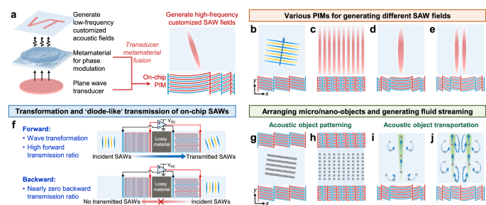
a Schematic of a PIM. Its mechanism is inspired by acoustic holography that uses a wave transformation module (e.g., a lens or metamaterial) containing required position-dependent phase information for modulating acoustic waves generated from a plane-wave transducer. Our PIM integrates the wave transformation and generation modules, by encoding the required subwavelength-resolution position-dependent phase information into the shapes of the microscale interdigital electrodes deposited on piezoelectric wafers. b−e Four different designs of PIMs for generating SAWs propagating a desired direction, pseudo-standing SAWs, a long SAW jet, and SAW twin jets, respectively. f Schematic illustrating the mechanism of a metamaterial that is based on a PIM for enabling the functions of transforming on-chip SAWs and “diode-like” transmission of SAW information. g, h Schematic illustrating the function of arranging micro-objects using the acoustic radiation force generated by a PIM. i, j Schematic illustrating the function of driving micro/nano-object motions using acoustic streaming generated by a PIM. The yellow and blue parallel lines in (b) and (f) represent SAW wavefronts, while the SAW intensity patterns in (a) and (b) are illustrated in red.
PIMs can also be used to develop SAW chips that transform incident SAWs and achieve “diode-like” unidirectional transmission of the information carried by SAWs. As illustrated in Fig. 1f, by integrating four key modules, including a typical straight-electrode IDT, a lossy material (e.g., high-damping paste or polymer), a gain module (e.g., one-way amplification circuit), and a PIM, we have developed a SAW metamaterial chip capable of transforming forward-propagating SAWs into waves with desired wavefronts and energy distributions. For example, when straight-wavefront SAWs incoming from the left side of the chip reach the straight-electrode IDT, an electrical signal is generated from the IDT. This signal is then amplified by a one-way amplification circuit and sent to the PIM on the right side of the lossy material. This allows the incident straight-wavefront SAWs to be transformed into SAWs with desired wavefronts and energy distributions, depending on the PIM’s electrode pattern. In contrast, the information of SAWs incoming from the right side of the metamaterial cannot be transmitted to the left side, as the amplification circuit ensures one-way transmission and amplification of the electrical signal. The lossy material is also critical to achieving “diode-like” unidirectional transmission of SAW information, as it absorbs SAWs arriving from both sides of the piezoelectric substrate and breaks the wave path through the substrate.
In addition to manipulating SAW propagation, PIMs can facilitate the development of acoustic tweezers for manipulating micro/nano-objects, as well as on-chip flow control devices that can generate versatile fluid streaming fields. On one hand, using a pair of PIMs, customized distributions of acoustic potential valleys can be generated to trap tiny objects using acoustic radiation forces and arrange them in various patterns, such as tilted parallel-line-like and two-dimensional (2D) lattice-like arrangements (Fig. 1g, h). With this design approach, infinite customized SAW energy patterns can be generated to construct diverse object patterns by carefully designing the electrode shapes of PIMs through the encoding of desired phase profiles. On the other hand, traveling SAWs from PIMs can generate acoustic streaming in a liquid layer on the SAW substrate, further inducing drag forces on tiny objects to transport them along streamlines. PIMs open a route for generating customized fluid streaming fields, as the PIMs’ electrode configurations can be engineered to generate various traveling SAW fields. For instance, a PIM designed to generate a long narrow SAW beam can produce a jet flow accompanied by multiple pairs of counter-chirality vortices on different sides of the jet flow (Fig. 1i). When customized to generate two long narrow SAW beams, two fluid jets accompanied by more pairs of counter-chirality vortices can be generated (Fig. 1j).
To support the development of PIMs, we established an analytical model (see Supplementary Note 1 and Supplementary Fig. 1) to quickly predict SAW fields generated by PIMs. Moreover, we have performed laser vibrometry-based SAW field visualization experiments to validate the ability of PIMs to generate SAWs with different wavefronts and energy patterns. Furthermore, using our PIMs, we have developed SAW metamaterial chips and experimentally validated their functions of transforming incident SAWs and performing “diode-like” transmission of SAW information. In addition, through a series of acoustofluidic experiments, we have demonstrated the capability of PIMs to generate acoustic streaming and arrange the distributions of micro/nano-objects. The key experimental results, along with the related data analysis and discussion, are given below.
Generation of versatile surface acoustic wave (SAW) fields
The shape of a PIM’s interdigital electrode is critical for generating SAWs with the desired frequency, wavefront shape, and energy pattern. Based on our proposed approach, which encodes the desired subwavelength-resolution spatially varying phase information into the electrode shape, we have developed multiple PIMs (see Supplementary Figs. 2 and 3 for configurations) to generate customized SAWs, such as tilted SAWs propagating in a desired direction and pseudo-standing SAWs. The mathematical descriptions of electrode shapes are provided in Supplementary Note 2. To characterize the PIMs, we acquired their generated SAW displacement and energy fields using a laser vibrometry system (Supplementary Fig. 4) and further analyzed the generated SAW field’s wavenumber spectrum in the kx-ky domain.
To generate SAWs propagating in a direction of eθ = (cos θ, sin θ) (illustrated in Supplementary Fig. 2a), the PIM’s electrode shape should be encoded with a spatial-varying phase profile having a constant gradient \(-\omega \,\cot \theta /{c}_{SAW}(\theta )\), where \(\omega\) is the angular frequency and \({c}_{SAW}(\theta )\) is a direction-dependent SAW velocity. For example, when using a PIM (illustrated in Fig. 2b) encoded with a gradient phase profile shown in Supplementary Fig. 3b (top), the laser-measured SAW displacement field in Fig. 2e shows tilted wavefronts perpendicular to the SAW propagation direction θ = 80 deg. This is also confirmed by the wavenumber analysis result in Fig. 2h, showing a high-intensity wavenumber spot in 80 deg in the kx-ky domain. In contrast, SAWs generated by a traditional straight-electrode IDT propagate in the 90 deg direction (Fig. 2d) and have a high-intensity wavenumber spot in 90 deg in the kx-ky domain (Fig. 2g). Additionally, the simulation results agree well with the experimental results (Fig. 2d–f), successfully validating our analytical model, which is for quickly predicting SAWs generated by PIMs with complex-shaped interdigital electrodes and guiding the PIM design and optimization.
Fig. 2: Experimental results for the generation of different high-frequency surface acoustic wave (SAW) fields on piezoelectric chips.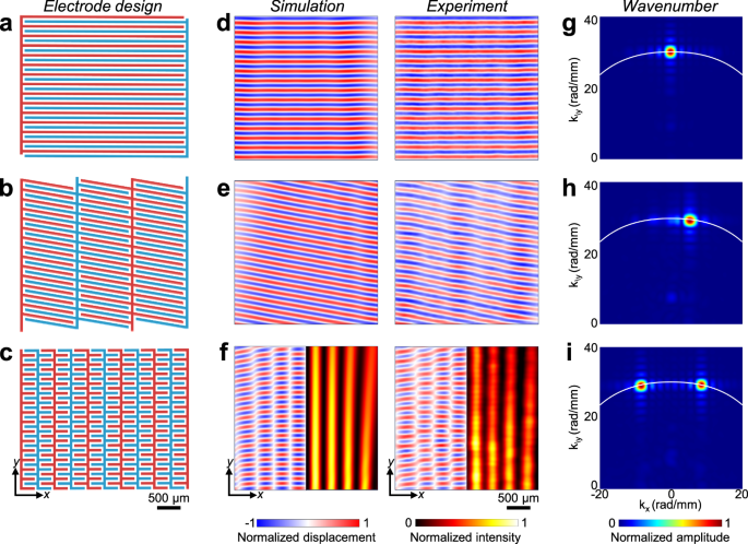
a−c Exact electrode configurations of different interdigital transducers (IDTs). d−f, left SAW fields simulated by our analytical model. d−f, right SAW fields experimentally acquired by a laser Doppler vibrometer. g−i Wavenumber spectra of the generated SAW fields. The white curves represent the theoretical wavenumber contour at 18.8 MHz. The first row gives the results of a traditional straight-electrode IDT. The second and third rows give results of phased interdigital metamaterials (PIMs) that can generate SAWs propagating in the 80 deg direction and pseudo-standing SAWs, respectively.
By encoding the electrode shape with a phase profile in Supplementary Fig. 3c, which alternates between 0 and π rad with a spatial period of ∆d, we developed a PIM to generate pseudo-standing SAWs. Details of the phase profile expression and PIM design can be found in Supplementary Note 2 and Supplementary Fig. 2b. For validation, we manufactured a PIM and performed laser-based SAW field characterization. The measured SAW intensity field (Fig. 2f, right) is similar to the intensity fields of standing SAWs generated by a pair of parallel IDTs, and thus the SAWs generated by our PIM are referred to as ‘pseudo-standing SAWs’ in this study. From the measured intensity field, it is evident that the x-direction spacing between adjacent intensity peaks is ∆d/2, which depends on the design of the PIM rather than the generated SAW’s wavelength (λ). Moreover, this spacing is the same as the peak spacing in regular standing SAWs created by the interference of SAWs carrying wavenumbers of ±2π/∆d generated at a frequency \(f={c}_{SAW}(\theta )/\varDelta d\). To further analyze the ‘pseudo-standing SAWs’, the acquired SAW field is transformed to a wavenumber spectrum in the kx-ky domain. The experimental wavenumber spectrum in Fig. 2i clearly shows two high-intensity spots symmetric to the ky-axis. Our experimental results in the x-y and kx-ky domains prove the effectiveness of generating ‘pseudo-standing SAWs’ using only a PIM to generate traveling SAWs propagating in one direction, rather than the traditional method of using multiple IDTs to generate counter-propagating SAWs.
Generation of long narrow surface acoustic wave (SAW) jets
In addition to generating SAWs propagating in a desired direction and pseudo-standing SAWs, we have developed and validated PIMs (illustrated in Fig. 3a–d) for generating single long SAW jets and twin jets. An acoustic jet is a highly focused acoustic beam with a long beam length in the wave propagation direction while maintaining a subwavelength-scale width68,69,70, which is defined by the distance between the beam’s full width at half maximum (FWHM) points illustrated in Supplementary Fig. 5. However, few methods can generate one or multiple long SAW jets on piezoelectric chips. Our developed PIMs overcome this limitation, enabling the generation of a long SAW jet and a pair of jets (i.e., twin jets) at high frequencies, such as tens of megahertz. Moreover, key parameters of a SAW jet, such as beam length, orientation, and center position, can be customized by carefully designing the PIM’s electrode configuration.
Fig. 3: Experimental results for the generation of different high-frequency surface acoustic wave (SAW) energy beams on piezoelectric chips.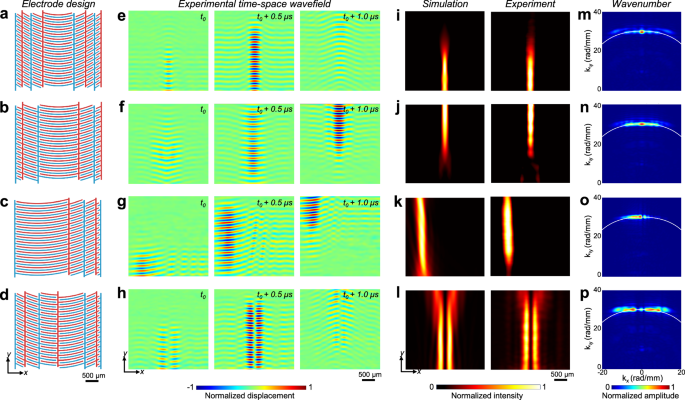
a−d Exact electrode configurations of the used phased interdigital metamaterials (PIMs). e−h Experimentally acquired on-chip SAW fields at different times after excitation. i−l, left SAW energy fields simulated by our analytical model. i−l, right SAW energy fields experimentally acquired by a laser Doppler vibrometer. m−p Wavenumber spectra of generated SAW fields. The white curves represent the theoretical wavenumber contour at 18.8 MHz. The first to fourth columns show the results of generating a long SAW jet near a PIM, a long SAW jet far from a PIM, an off-center SAW jet, and twin jets, respectively.
The key to generating a long SAW jet is to optimize the PIM’s electrode shape so that the PIM can generate a series of focused SAWs whose focal points gradually change from xF(1) to xF(N) as illustrated in Supplementary Fig. 5. Using this approach, a long SAW jet with an energy profile ranging from xF(1) to xF(N) can be generated, as confirmed by the alignment of the generated SAW jet with the focal points shown in Supplementary Fig. 6. Moreover, SAW jets can exhibit different shapes by customizing PIM design parameters (e.g., the number of electrodes N, device span W, focal length dc, and beam center shift Δs), as demonstrated by the simulation results in Supplementary Fig. 7, which also reveal how these parameters affect beam width (Wb). The results show that the beam width gradually increases with increasing focal length and/or decreasing device span. When the number of electrodes is small (e.g., N = 2), this relationship aligns with the prediction Wb = 1.02 λ dc/ Wc, which is commonly used to estimate the beam widths of focused ultrasound transducers77,78. Second, shifting the jet away from the device centerline toward the edge (i.e., increasing Δs) results in a gradual increase in beam width. Third, as the number of electrodes increases, the beam width initially increases and then reaches a plateau. Additionally, by appropriately selecting the design parameters, subwavelength-scale beam widths can be achieved. These relationships observed from simulation results provide valuable guidance for optimizing PIM designs.
For experimental validation, we fabricated three PIMs, whose electrode shapes were designed based on phase profiles in Supplementary Fig. 3d–f, for generating single long SAW jets with different energy distributions (see Fig. 3a–c). When using a PIM (Fig. 3a) designed with focal points close to its electrodes, the measured SAW displacement and energy fields (Fig. 3e, i) clearly show a long SAW jet near the electrodes along the PIM’s centerline. When using a PIM (Fig. 3b) designed with focal points far from the electrodes, a long SAW jet far from the PIM electrodes is generated, as shown by the measured SAW displacement and energy fields (Fig. 3f and j). We also showed the ability to generate an off-center SAW jet (see Fig. 3g and k) by using a PIM whose focal points offset from the PIM centerline. To further analyze the generated SAW jets, the multi-dimensional Fourier transform was applied to the acquired wavefields to reveal their wavenumber components. Compared to the unfocused SAW’s spectrum (Fig. 2g) with only a high-intensity spot, the SAW jets generated along the centerline have wavenumber components widely and symmetrically spread in the ±kx directions (Fig. 3m, n). When a SAW jet is left shifted, its spectrum becomes asymmetric with higher intensity in the region with kx < 0 (Fig. 3o).
In addition to demonstrating single SAW jets, we fabricated a PIM (Fig. 3d) capable of generating a pair of long, narrow jets (referred to as twin jets), which, to the best of our knowledge, has not been achieved before. This PIM minimizes the SAW energy along the centerline through destructive interference, thus allowing for splitting a SAW jet into two lobes to create twin jets. Here, energy minimization is achieved by introducing an additional phase change of π rad to half of the PIM originally designed to generate a single SAW jet. The experimental SAW intensity field in Fig. 3l (right) confirms the generation of a pair of slim SAW jets (i.e., twin jets) with a low energy region confined between them. The wavenumber spectrum in Fig. 3p for twin jets shows two high-intensity regions that are nearly symmetric to the ky-axis, in contrast to the single jet’s wavenumber spectrum in Fig. 3m. Additionally, we found that after splitting a single jet into twin jets, the width of each split jet becomes smaller than that of the original. However, as the device span increases, this effect gradually diminishes, as shown in Supplementary Fig. 7l.
The above analytical and experimental results demonstrate the ability to generate a single long SAW jet and twin jets using PIMs whose electrode shapes are encoded with customized spatial-varying phase profiles. Moreover, by optimizing the interdigital electrode configuration, PIMs can be developed to generate SAW jets with customized beam lengths and positions. Furthermore, compared to a traditional focused IDT with concentric arc-shaped electrodes, a PIM with the same span (W), number of electrodes (N), and center electrode focal length (dc) can generate a significantly longer focused SAW beam, although its width slightly increases, as shown in Supplementary Fig. 8. Additionally, the four SAW fields (Fig. 3i–l, left) simulated using our analytical approach described in Supplementary Note 1 closely resemble their corresponding experimental SAW fields (Fig. 3i–l, right). The beam widths measured from the experimental SAW fields are also close to those obtained from the simulation results (see Supplementary Fig. 9 for beam width comparisons), except for the case in Fig. 3k, which may be attributed to SAW field measurement and device fabrication errors. These results indicate that our analytical model is effective in predicting complex SAW jets generated by PIMs, thereby facilitating the design of PIM devices.
Transformation and ‘diode-like’ transmission of on-chip surface acoustic waves (SAWs)
Acoustic metamaterials are attracting increasing attention for transforming incident acoustic waves by modulating the phase and amplitude profiles of waves transmitted through them, as well as for achieving “diode-like” transmission of acoustic waves, i.e., one-way routing79,80,81,82. However, most studies focus on manipulating low-frequency acoustic waves such as bulk waves in air, fluids, and solids. Few studies have realized metamaterials capable of transforming the energy field of SAWs into desired patterns. Moreover, few studies have developed metamaterials that can both transform on-chip SAWs and achieve “diode-like” wave transmission.
To address these limitations, we have developed SAW metamaterial chips (illustrated in Fig. 1f) that can both transform incident SAW fields into desired patterns and achieve ‘diode-like’ routing. Our SAW metamaterial chip is composed of four key modules: (i) a straight electrode IDT, (ii) a lossy material (e.g., high-damping paste or polymer) bonded on the substrate for absorbing SAWs as proven by experimental results in Supplementary Fig. 10, (iii) a one-way gain module (e.g., amplification circuit) for signal amplification and breaking symmetry, as well as (iv) a PIM for emitting transformed SAWs. In the forward direction, an incident SAW is first received by the left-side straight-electrode IDT, generating an electrical signal that is amplified by the one-way gain module. The amplified voltage signal is then sent to the PIM to emit a transformed SAW to the right side of the chip. Through this process, an incident SAW can be transformed into a SAW with the desired wavefront/energy pattern, which depends on the PIM design. In the backward direction, a SAW incoming from the right side of the chip is first received by the PIM, producing an electrical signal. However, this signal cannot be delivered to the left-side straight-electrode IDT, due to the one-way amplification circuit. In addition, the SAW propagating in the −y-direction cannot transmit through the piezoelectric substrate to the left side of the chip because the on-substrate high-damping lossy material absorbs SAWs.
For validation, we fabricated and characterized three SAW transformation chips having different PIM designs (see Fig. 4a, c, and e). When using the design in Fig. 4a, the acquired SAW displacement fields in Fig. 4b and Supplementary Movie. 1 reveal that incident SAWs propagating in the +y-direction can be steered to a direction 10 deg off the +y-axis. When using the chip design in Fig. 4c, the incident straight-wavefront SAWs are transformed into a focused SAW jet, as shown by the acquired displacement fields in Fig. 4d and Supplementary Movie. 2. Moreover, using the chip design in Fig. 4e, the incident SAWs are transformed into twin jets, as shown in Fig. 4f and Supplementary Movie. 3. In addition, the “diode-like” SAW transmission capability has been validated. The acquired SAW displacement fields in Fig. 4h and Supplementary Movie. 4 show that SAWs generated on the right side of the chip cannot transmit to the left side. The acquired transmission spectra in Supplementary Fig. 11 further confirm the ‘diode-like’ high transmission in the forward direction and nearly zero transmission in the backward direction. By reversing the amplification circuit, backward high transmission can be achieved, while prohibiting forward transmission. Therefore, as validated by our experimental results in Fig. 4 and Supplementary Fig. 11, our developed SAW metamaterial chips enable the transformation of incident SAW fields into desired patterns, as well as the ‘diode-like’ delivery of the information carried by SAWs. Additionally, since the chip uses an IDT positioned to the left of the lossy material for SAW sensing, a small portion of the incident SAW energy ( ~ 9.3%, according to experimental results) is reflected. The IDT’s inherent filtering capability allows for frequency-selective SAW transmission. By replacing the sensing IDT with differently shaped sensing electrodes, it may be possible to reduce SAW reflections and enable multi-frequency or broadband SAW transmission — an interesting direction for future investigation.
Fig. 4: Results of transforming incident surface acoustic waves (SAWs) into waves with different wavefronts and energy patterns.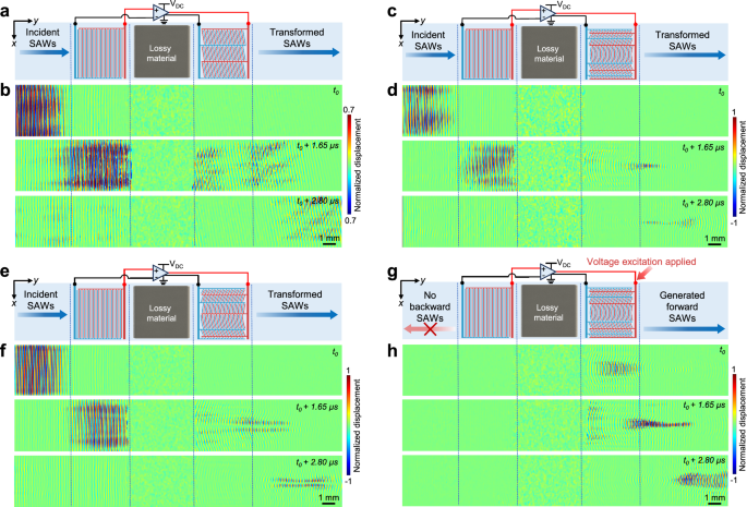
a Chip design and (b) acquired SAW fields for steering straight-wavefront SAWs propagating in the +y-direction to a direction 10 deg off the +y-axis. c Chip design and (d) acquired SAW fields for transforming straight-wavefront SAWs to a focused SAW jet. e Chip design and (f) acquired SAW fields for transforming straight-wavefront SAWs to twin jets. g Chip design and (h) acquired SAW fields showing that backward transmission of SAWs is prohibited.
Phased interdigital metamaterials (PIMs) for acoustofluidics
Acoustofluidics has shown great potential for generating and controlling fluid flows, as well as arranging and transporting micro/nano-objects in fluids. In recent years, these acoustofluidic abilities have been increasingly used for developing lab-on-a-chip devices for biomedical research and applications such as rotating cells, separating bioparticles, concentrating exosomes, as well as transporting and mixing biofluids14,15,16,17,18,19,20,21,22,23,24,25. Here, we demonstrate that our PIMs can be used for acoustofluidics by enabling acoustic streaming to manipulate fluids and applying forces on micro/nanoparticles to transport and arrange them. The acoustofluidic experiments were performed using setups illustrated in Supplementary Fig. 12, with particle distributions and motions recorded by a camera.
When using a pair of PIMs for generating tilted standing SAWs, the acquired microscopic image in Fig. 5b and Supplementary Movie. 5 show that 35 μm SiO2 particles are arranged in a tilted, parallel-line-like distribution, as these microparticles are trapped by the potential valleys of the generated tilted standing SAWs. Interestingly, microparticles can be arranged in a 2D lattice-like pattern (see Fig. 5e and Supplementary Movie. 6), when using a pair of PIMs designed for generating pseudo-standing SAWs. Previous approaches for constructing 2D lattice-like particle patterns typically required orthogonally arranged IDTs that generated SAWs propagating along orthogonal axes; however, our PIM-based approach requires only SAWs propagating along a single axis, which has not been presented before to the best of our knowledge. Since SAWs generated on a piezoelectric wafer are accompanied by dynamic electric fields, we also demonstrated the ability of our PIMs for arranging MWCNTs using the accompanied electric fields. When using tilted standing SAWs, MWCNTs align perpendicular to the node lines, forming multiple parallel groups in the potential valleys of the tilted standing SAWs, as shown by the acquired microscopic image in Fig. 5c. When using pseudo-standing SAWs, MWCNTs align along the SAW propagation direction, forming multiple groups (see Fig. 5f) in SAW potential valleys with a 2D lattice-like distribution. Additionally, the arrangements of microparticles and MWCNTs observed in the above experiments can be predicted using analytically simulated SAW-induced acoustic radiation and dielectrophoretic force fields, respectively (see Supplementary Note 1 and Fig. 13 for the simulation approach and results, respectively).
Fig. 5: Experimental results showing acoustofluidic phenomena achieved by phased interdigital metamaterials (PIMs).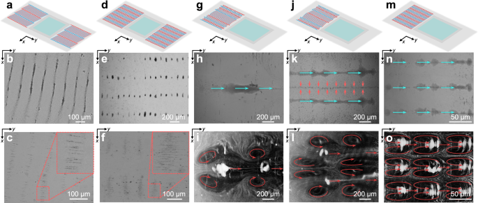
a Chip design and (b, c) results of patterning 35 μm SiO2 microparticles and multi-walled carbon nanotubes (MWCNTs) using tilted standing surface acoustic waves (SAWs) generated by a pair of PIMs. d Chip design and (e, f) results of patterning microparticles and MWCNTs using pseudo-standing SAWs generated by a pair of PIMs. g Chip design and (h, i) results of transporting 35 μm and 550 nm SiO2 microparticles using a focused SAW energy beam. j Chip design and (k, l) results of transporting 35 μm and 550 nm SiO2 microparticles using a pair of focused SAW beams. m Chip design and (n, o) results of transporting 35 μm and 550 nm SiO2 microparticles using three energy beams of pseudo-standing SAWs.
In addition to arranging the distributions of micro/nano-objects, we demonstrated the ability to transport particles, as well as generate unique fluid streaming fields. First, when using a PIM to generate a long narrow SAW beam, Fig. 5h and Supplementary Movie 7 show that 35 μm SiO2 particles were transported along the SAW beam, primarily by the acoustic radiation force. The acoustic streaming pattern (Fig. 5i), observed through 500 nm SiO2 particles influenced mainly by the streaming-induced drag force, revealed a microscale jet flow accompanied by multiple pairs of counter-chirality vortices symmetric to the jet (Supplementary Fig. 14d and Movie. 8). Interestingly, this flow pattern resembles the classical free in-air subsonic jet with an array of vortices83, but here it is observed in a microscale liquid environment on a piezoelectric chip. Second, when using a PIM to generate two long narrow SAW beams, 35 μm particles were transported along the two SAW beams (see Fig. 5k and Supplementary Movie. 9), with some microparticles trapped along the centerline between the two SAW beams due to minimal SAW potential from destructive interference. The streaming pattern (Fig. 5l) revealed by 500 nm particles shows that each high-potential SAW beam induced a forward flow with counter-chirality streaming vortices on different sides, and interestingly, the combined effect of inner vortices created a backward flow along the low-potential centerline between the two SAW beams (Supplementary Fig. 14e and Movie. 10). Third, when using a PIM to generate pseudo-standing SAWs with multiple high-intensity beams, 35 μm particles were transported by these high-intensity beams (Fig. 5n and Supplementary Movie. 11). Moreover, each SAW beam induced a forward streaming flow with multiple pairs of counter-chirality streaming vortices on different sides (Supplementary Fig. 14f and Movie. 12). Their combination created an array of periodically arranged streaming vortices (Fig. 5o), having the same chirality along the +y-direction and alternating chirality in the +x-direction.