
Engineering H
ex by using heavy metals
We first studied the Co/Ru/Co trilayer structure with IEC and investigated the influence of the PMA of the top Co layer on the magnetization process. To tune the PMA, we deposited ultrathin Ir (0–0.28 nm)/MgO on the top Co layer. In our previous studies on the Co/ultrathin Ir (0–0.1 nm)/MgO structure, PMA of the Co layer is largely enhanced by increasing the thickness of the Ir layer32,33. Thus, we prepared substrate/seed/buffer layers/Co (1.1 nm)/Ru spacer (0–0.9 nm)/Co (1.1 nm)/ultrathin Ir (0–0.28 nm)/MgO (3 nm)/indium tin oxide (20 nm) polycrystalline film on a thermally oxidized silicon substrate (Fig. 2a and Methods). The magnetic properties of the multilayer films were evaluated by the polar magneto-optical Kerr effect (p-MOKE; Fig. 2b and Supplementary Note 1).
Fig. 2: IEC in Co/Ru/Co trilayer structure.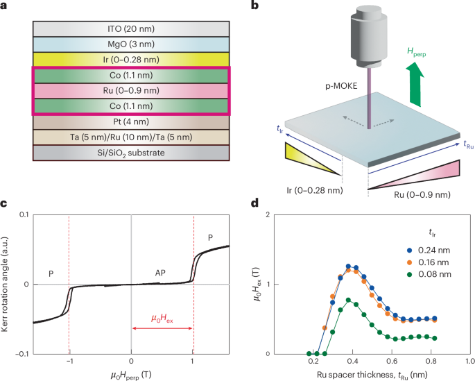
a, Schematic of the multilayer structure for IEC measurements. b, Schematic of the measurement configuration for p-MOKE. c, Typical p-MOKE magnetization curve of Co/Ru/Co trilayer, where Ru thickness (tRu) is 0.35 nm and Ir thickness (tIr) is 0.11 nm. Switching from the AP to P configuration takes place at the exchange field (Hex) of the IEC. d, μ0Hex plotted as a function of tRu for various tIr values.
Figure 2c shows a typical p-MOKE magnetization curve for Co/Ru/Co with tRu = 0.35 nm and tIr = 0.11 nm, which exhibits an antiferromagnetic IEC, measured under a magnetic field applied perpendicular to the film plane (Hperp). When |Hperp| > Hex is applied, the magnetic state switches from the AP to P configuration. The magnetization curve is discussed in more detail in Supplementary Note 2. Because the switching of magnetization configuration is accompanied with a hysteresis loop, we define the centre of the hysteresis loop as Hex. Hereafter, we focus on positive magnetic fields for simplicity because the magnetization process is symmetric with respect to Hperp. We investigated the Ru thickness (tRu) dependence of Hex in Co/Ru/Co because the magnitude of Hex is known to exhibit oscillatory behaviour with respect to tRu (ref. 26). In Fig. 2d, Hex is plotted as a function of tRu. Here the first peak appears at tRu ≈ 0.4 nm, which is consistent with our previous work on Co-based multilayers and Ru spacer27. An increase in tIr, which causes an increase in the PMA of top Co layer, tends to increase Hex. Note that the data for tIr = 0 nm is not shown because the magnetization of Co is aligned in the film plane. Hex increases with respect to tIr and tends to saturate when tIr ≥ 0.16 nm. These results suggest that tIr < 0.16 nm will be suitable for controlling Hex by voltage.
The maximum value of the effective exchange coupling energy Jex = μ0HexMStCo* is evaluated to be 1.8 mJ m−2, where μ0 is the permeability of vacuum, tCo*(≡tCo − tdead) is the effective thickness of the Co layers, supposing that the saturation magnetization MS of Co is 1,417 kA m−1, the thickness of Co layers (tCo) is 1.1 nm, and the thickness of the magnetically dead layer (tdead) is 0.1 nm (refs. 33,34). This Jex value is comparable with the value reported in our previous work27.
Voltage control of H
ex
To study VCMA-driven phenomena, we fabricated the multilayer film shown in Fig. 2a into a device structure schematically illustrated in Fig. 3a by using typical microfabrication techniques. The lateral size of the VCMA junction in Fig. 3a is 10 × 8 μm. Figure 3b shows the typical p-MOKE magnetization curves of Co/Ru/Co trilayer with tRu = 0.34 nm and tIr = 0.11 nm in the vicinity of μ0Hex for applied bias voltages with different polarities. When a negative (positive) voltage is applied to the device, PMA and Hex increase (decrease) due to the VCMA effect. These behaviours are consistent with the results shown in Fig. 2. As shown in Fig. 3c, Hex linearly decreases with the applied bias voltage (Vbias), which is also consistent with the sign of the VCMA effect. The negative slope shown in Fig. 3c (–Δμ0Hex/Vbias) is the efficiency of the voltage control of Hex.
Fig. 3: Voltage-controlled effective Hex based on VCMA effect.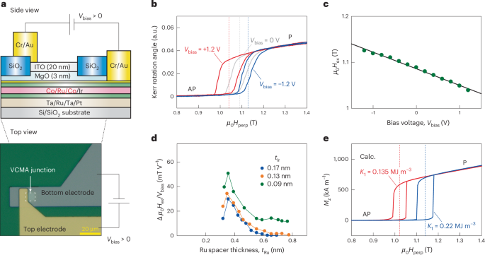
a, Schematic and photograph of the device structure for studying the VCMA-driven phenomena. b, Bias-voltage-dependent p-MOKE magnetization curves in the vicinity of μ0Hex, where tRu = 0.34 nm and tIr = 0.11 nm. c, Vbias dependence of μ0Hex. d, Efficiency of the voltage control of Hex, Δμ0Hex/Vbias, plotted as function of tRu. e, Calculated magnetization curves. Although J is constant, the effective Hex depends on the PMA energy of the top Co layer (K1).
To efficiently control Hex by means of voltage, we optimized the multilayer structure. Figure 3d plots the tRu dependence of Δμ0Hex/Vbias for various tIr values. Large Δμ0Hex/Vbias was obtained in the vicinity of the first peak of Hex near tRu = 0.4 nm (Fig. 2d). The largest value of Δμ0Hex/Vbias is about 52 mT V−1, which corresponds to the efficiency of the effective VCEC, defined as (ΔJex/ΔVbias) × tbarrier = (Δμ0HexMStCo*/ΔVbias) × tbarrier, of −180 fJ V−1 m−1, where tbarrier is the thickness of the tunnel barrier. Surprisingly, this value is two orders of magnitude larger than the largest value reported in previous studies on the VCEC effect31, clearly suggesting that the VCMA effect is an effective way for tuning the effective IEC by voltage. It should be noted that the physical origins of the VCEC effect observed in previous studies14,15,18,29,31 are different from the VCMA effect. The term VCEC is not strictly correct in this study because the IEC is not directly controlled by voltage but is effectively tuned by the VCMA effect.
To understand the observed effective voltage-controlled IEC in more detail, we conducted macrospin calculations on the magnetization curves of an artificial antiferromagnetic trilayer (Supplementary Note 5). Figure 3e shows the magnetization curves of the artificial antiferromagnetic trilayer with different PMA energies of the top Co layer (K1). Here the PMA energy of the bottom Co layer (K2), interlayer exchange coupling constant (J), saturation magnetization of Co layers and thickness of Co layers are fixed at 0.185 × 10⁶ J m−3, −3.25 × 10⁻³ J m−2, 1,400 kA m−1 and 1.0 nm, respectively. The Gilbert damping constants were set to 1.0 to reduce the computation time. The tendency of the experimental results that Hex increases (decreases) with increasing (decreasing) PMA of the top Co layer (Fig. 2d) is reproduced by the calculations. Even though the exchange coupling constant J remains unchanged, the effective Hex is tuned by the PMA of the top Co layer. The important point here is that the effective Hex can be manipulated solely by voltage. Because Hex largely depends on the applied voltage, we can expect voltage-induced bidirectional magnetization switching under a fixed magnetic field. It should be noted that the macrospin model cannot account for the spatial inhomogeneity of magnetization or domain nucleation. Therefore, the model is not applicable to systems exhibiting multidomain formation. Large-scale micromagnetic simulations would be required for a fully quantitative comparison with experiments, as they are essential for accurately capturing the non-uniform magnetization dynamics observed in real devices.
We also studied junctions with the opposite sign of the VCMA effect (Supplementary Note 3). By changing the materials and stacking structure of the multilayer samples, we inverted the sign of the VCMA effect and observed the inversion of the slope of μ0Hex–Vbias relationship (Supplementary Fig. 3c). This is additional evidence that the origin of the voltage-controlled effective Hex and Jex is the VCMA effect.
VCMA-SMS
To effectively demonstrate VCMA-SMS, we first tried to enhance the VCMA and the voltage-controlled Hex by using MgO (2 nm)/HfOx (5 nm) as the insulating tunnel barrier layer which has a larger dielectric constant (Fig. 4a and Methods)35. Figure 4b shows the magnetization curves in the vicinity of μ0Hex, where tRu = 0.39 nm and tIr = 0.10 nm. The Vbias dependence of μ0Hex (Fig. 4c) corresponds to a VCEC efficiency of −310 fJ V−1 m−1, which is substantially higher than that of the samples in Fig. 3 (−180 fJ V−1 m−1). The enhanced voltage-controlled Hex and Jex are attributed to the larger VCMA effect. Compared with the voltage-dependent hysteresis loops shown in Fig. 3b, the hysteresis loops for positive and negative voltages shown in Fig. 4b are clearly separated from each other. This indicates that the magnetization configuration can be switched solely by voltage when the magnetic field is fixed at the centre of these hysteresis loops. We also fabricated devices with the same structure and nominal film thickness on different substrates and evaluated the variation in μ0Hex. Even among different deposition batches, the device-to-device variation in μ0Hex remains small, with a standard deviation of approximately 4 mT. Such a variation in μ0Hex does not pose a serious problem for the write operation in the present scheme.
Fig. 4: Experimental demonstration of VCMA-SMS.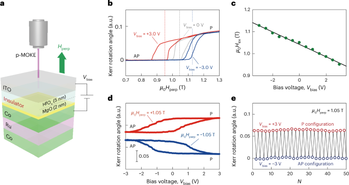
a, Schematic of the experimental configuration with p-MOKE measurement. To enhance the VCMA, we used a hybrid insulating barrier with a high-k material HfOx. b, p-MOKE hysteresis curves of the multilayer device, where tRu and tIr are 0.39 nm and 0.10 nm, respectively. c, Vbias dependence of μ0Hex. d, Vbias dependence of p-MOKE signal under fixed μ0Hperp with different polarities. e, Change in p-MOKE signal by alternately applying positive (N = 1, 3, 5…) and negative (N = 2, 4, 6…) Vbias.
Figure 4d shows the experimental results of purely voltage-induced magnetization switching under a fixed magnetic field. A clear hysteresis loop was observed at μ0Hperp = +1.05 T. At Vbias = 0, the magnetization configuration exhibits bistable states corresponding to the AP and P configurations. This is a successful demonstration of VCMA-SMS. A similar VCMA-SMS takes place at μ0Hperp = –1.05 T. We repeated VCMA-SMS to confirm its reliability. Positive and negative voltages (±3 V) were alternately applied by sweeping the voltage. To observe purely voltage-induced effects, here we used a thick insulating layer with a thickness of 7 nm, which leads to a high electrical resistance (~1 GΩ). The maximum charge current density is less than 38 A m−2, which is several orders of magnitudes smaller than that for STT switching. Figure 4e shows the p-MOKE signal for Co/Ru/Co at positive (N = 1, 3, 5…) and negative (N = 2, 4, 6…) voltages, where N represents the cycle index. Repeatable switching events were confirmed with d.c. voltages. In Fig. 4e, the p-MOKE signal for AP and P configurations slightly varies at each switching event. This suggests that the junction sample with a large lateral size (10 × 8 μm) does not have a perfectly single magnetic domain. Such variation will be eliminated simply by shrinking the sample area to approach a single-domain state.
VCMA-SMS with short voltage pulses
Next, we demonstrate VCMA-SMS by applying short voltage pulses to the same sample and prove its applicability to high-speed memory devices. Here we performed p-MOKE measurements after applying voltage pulses with pulse widths of tens of nanoseconds. It should be noted that voltage pulses in this width range can easily be controlled in large-scale memory chips with circuit delay. Note also that voltage pulses with such widths cannot induce the conventional VCMA-induced dynamic switching8,10. To apply short voltage pulses, we used an arbitrary function generator. Before the measurements, a magnetic field of +1.8 T was applied to initialize the magnetic configuration at the P state. We measured the p-MOKE signals before and after applying voltage pulses at fixed Hperp of +1.05 T.
We first show the experimental result for the pulse width of 75 ns. Figure 5a shows the p-MOKE signals after the application of negative (N = 1, 3, 5…) and positive (N = 2, 4, 6…) voltage pulses. Repeatable switching events were demonstrated with the voltage pulse as in the case of d.c. voltage. It should be noted that the p-MOKE signal for the P state (Fig. 5a) is slightly smaller than that in Fig. 4e. This is mainly because p-MOKE shown in Fig. 5a was measured after the voltage was removed, whereas p-MOKE shown in Fig. 4e was measured under the applied voltage.
Fig. 5: VCMA-SMS by voltage pulse.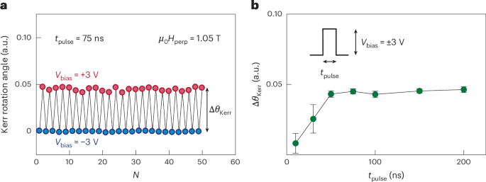
a, Change in the p-MOKE signal by alternately applying negative (N = 1, 3, 5…) and positive (N = 2, 4, 6…) voltage pulses with a pulse width of 75 ns. b, Change in p-MOKE signal between the AP and P states (ΔθKerr) due to VCMA-SMS as a function of the voltage pulse width (tpulse). Here the plotted values represent the mean ± s.d., both calculated from 50 measurements performed on the same sample shown in a.
Next, we conducted similar experiments with different pulse widths to investigate how fast the magnetization can be switched. Figure 5b plots the average change in the p-MOKE signal between the AP and P states (ΔθKerr) due to VCMA-SMS as a function of the voltage pulse width (tpulse). Reliable VCMA-SMS was observed with tpulse down to 50 ns, below which switching was imperfect. Reliable pulse-voltage-induced VCMA-SMS has been experimentally demonstrated in pulse widths ranging from 50 ns to ∞ (d.c. voltage).
Although VCMA-SMS with a pulse width of 50 ns is potentially applicable to voltage-controlled MRAM for embedded non-volatile memory, the optimum pulse width in terms of operation speed, circuit design and power consumption of non-volatile working memory is about 5–10 ns (ref. 1). Note that a pulse width of 5–10 ns is too long to induce the conventional VCMA-driven dynamic switching8,10. Here we discuss whether VCMA-SMS can be induced in this pulse width range. We should first emphasize that the observed VCMA-SMS with the pulse width of 50 ns is rather surprising because the sample is large (10 × 8-μm2-sized junction) and, therefore, is not a single magnetic domain. In the case of STT switching and VCMA-driven dynamic switching, such large junctions do not exhibit reliable switching because a single-domain state is essential for these types of switching. As the junction size shrinks below 100 nm and the magnetic state approaches a single-domain state, the junction generally shows more reliable and faster switching. To theoretically confirm this point, we performed a macrospin simulation of VCMA-SMS by assuming a single-domain state. We found that the minimum pulse width for inducing VCMA-SMS, tsw, becomes shorter as the Gilbert damping of the ferromagnetic layer increases. This relationship between magnetic damping and switching speed is similar to that for magnetic-field-induced switching used in magnetic recording devices such as hard disc drives, in which the magnetic media with high damping materials are used for faster writing. Our macrospin simulation with a damping constant of α = 0.05–0.1, which is reasonable for ferromagnetic alloys based on Fe–Pt and Co–Pt, showed that tsw can be shorter than about 1 ns. The macrospin simulation assumes a single-domain state. A single-domain state can be realized in MTJs with perpendicular magnetization when the junction diameter is smaller than 100 nm. By using such small junctions, we can expect reliable VCMA-SMS in the wide range of pulse widths from 1 ns to d.c. voltage.