
First-principles calculations
All calculations utilize the Vienna ab initio software package (v. 6.2.0), which implements the projector augmented-wave formalism of density functional theory43,44,45,46. We perform non-spin-polarized calculations using the PBEsol functional and standard projector augmented-wave potentials from the Vienna ab initio software package potential library: Sr_sv (4s24p65s2), Ba_sv (5s25p66s2), Ti_sv (3s23p63d24s2) and O (2s22p4). Wave functions are expanded up to an energy cut-off of 550 eV, and reciprocal space is sampled on an 8 × 8 × 1 Monkhorst–Pack grid (8 × 8 × 8 for a perovskite unit cell). We use an electronic convergence criterion of 10−8 eV.
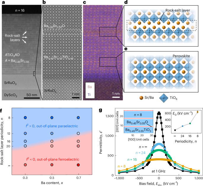
Conventional RP unit cells with n = 8, 12, 16 and 20 are constructed by extrapolation of the c-axis lattice parameter from cells with lower n and the insertion of alternating layers of TiO2 and SrO or BaO in accordance with space group symmetry I4/mmm. Lattice parameters and internal atomic coordinates are allowed to relax until the forces on all atoms are below 5 × 10⁻⁴ eV Å−1, simulating strain-free thin films. The target compositions of x = 0.3, 0.5 and 0.7 are approximated as closely as possible for each value of n. Several different cation configurations are sampled, and cation ordering is found to have only a minor effect on the calculated phonon frequencies.
Phonons are calculated at the Γ point for the non-polar (I4/mmm) structures. We used the finite displacement method as implemented in Phonopy (v. 2.12.0)47,48 with Vienna ab initio software package as the force calculator. All structures show dynamical instabilities, manifested as imaginary eigenvalues of the dynamical matrix, with the most strongly unstable mode being a polar phonon with Eu symmetry. This mode takes the structure to space group F2mm with in-plane polarization along [110] referred to the conventional unit cell49. For structures with sufficiently high n and x, an unstable polar phonon of A2u symmetry is also found, leading to polarization along [001] and space group I4mm if taken alone. The combination of in-plane and out-of-plane polarization leads to space group symmetry Cm.
Phase-field simulations
We use the dynamical phase-field method to simulate the polarization dynamics and dielectric tunability. The evolution of the polarization is governed by the polarization dynamics equation
$${\mu }_{{ij}}\frac{{\partial }^{2}{P}_{j}}{\partial {t}^{2}}+{\gamma }_{{ij}}\frac{\partial {P}_{j}}{\partial t}=-\frac{\delta F}{\delta {P}_{i}},$$
(1)
where μij is the polarization effective mass and γij is the polarization damping coefficient. We performed the simulations in the low-loss limit, where the damping coefficient (γij) has minimal role in the dielectric response. F is the total free energy, which is expressed as the integral over volume of the following energy densities:
$$F=\int {f}_{{\rm{Landau}}}+{f}_{{\rm{Elastic}}}+{f}_{{\rm{Electric}}}+{f}_{{\rm{Gradient}}}{\rm{d}}{V}.$$
(2)
We elaborate the individual contributions in Supplementary Section 1. At 1 GHz, damping has minimal impact on the dielectric response, as we perform the simulations in the low-loss limit. We confirmed this limit with frequency-dispersion simulations (Supplementary Fig. 14). The description of dielectric loss of the perovskite may be incomplete in the current phase-field model. Dielectric loss originates from both intrinsic and extrinsic mechanisms. Intrinsic losses arise from anharmonic interactions between phonons and viscous damping, whereas extrinsic losses arise from the motion of charged defects and the presence of local polar regions50. The dynamical phase-field method primarily captures the dynamics of the ferroelectric soft mode and the acoustic modes through the polarization-dynamic and elastodynamic equations51. Although the current simulations incorporate the intrinsic loss to some extent by accounting for viscous damping and some of the interactions between the soft-mode and acoustic modes, they omit extrinsic contributions, such as defect dynamics and potential local polar regions. Additional loss could transform the predicted under-dampened terahertz resonance (Supplementary Fig. 14) to the overdampened gigahertz relaxation that we observed in the experiment (Fig. 4a,b).
Finally, we evaluated the tunability by fitting the permittivity as a function of voltage with a model of field-induced hopping of random, non-interacting dipoles in a double-well potential52:
$$\varepsilon \left(E\right)={\varepsilon }_{\infty }+\Delta \varepsilon {\text{ sech}(E/{E}_{0})}^{2},$$
(3)
with real parameters ε∞ > 0, Δε > 0 and E0 > 0. The parameter E0 describes the width of the tuning peak.
Film growth
We grew the films in a Veeco Gen10 using conventional effusion cells for barium and strontium, an electron-beam evaporator for ruthenium and a Ti ball for titanium53. XRD and reciprocal space map measurements were performed with a PANalytical Empyrean Diffractometer. We used a substrate temperature of 650 °C for SrRuO3 and 770 °C for (ATiO3)nAO (measured by an optical pyrometer operating at a wavelength of 980 nm). We chose 50-nm-thick bottom and 25-nm-thick SrRuO3 top electrodes, which have a similar lattice parameter to our dielectric, because epitaxial electrodes reduce any parasitic interfacial series capacitance. We grew the MIMs on (110)-oriented DyScO3 substrates because its lattice parameter is almost perfectly lattice matched to our active layers: −0.1% mismatch to Ba0.45Sr0.55TiO3 and +0.6% mismatch to SrRuO3. To grow these phases on SrRuO3, in situ reflection high-energy electron diffraction was essential to accommodate ruthenium deficiency near the surface of the SrRuO3 electrode (Supplementary Section 2). We deposited the SrRuO3 layers in a background pressure of 1 × 10⁻⁶ torr of 80% O3 + 20% O2 and (ATiO3)nAO layers in a background pressure of 5 × 10⁻⁷ torr of 10% O3 + 90% O2. For SrRuO3, we supplied a ratio of 1Sr:3Ru and utilized the volatility of RuOx at the substrate temperature (650 °C) to thermodynamically control the stoichiometry of the electrode54. After depositing the SrRuO3 back electrode, we cooled the samples to room temperature and stored them in vacuum for ~1 week. We then returned the samples to the growth chamber; heated them to 500 °C in 5 × 10⁻⁷ torr of 10% O3 + 90% O2; and supplied (1) one monolayer of TiO2, (2) one monolayer of SrO and (3) one additional monolayer of TiO2 to the growth surface to encapsulate volatile RuOx before heating to 770 °C to complete the growth of (ATiO3)nAO.
Our method for growth of (ATiO3)nAO has been detailed previously21,55, but we offer a brief summary here. Between (AO)2 layers, we monitored the √2 × √2 surface reconstruction with in situ reflection high-energy electron diffraction to monitor the surface stoichiometry as we alternately supplied monolayers of AO and TiO2 such that the surface oscillated between termination with one monolayer of AO and termination with two monolayers of AO (ref. 21; see the loop shown in Supplementary Fig. 10a). Each AO monolayer was supplied by codepositing flux-matched strontium and barium sources for most of the layer (~9 s) and briefly closing the barium shutter in the middle of the monolayer (~2 s) to hit the target stoichiometry (45% barium). To crystallize a horizontal rock-salt layer at this substrate temperature, the growth front must be terminated with three AO layers24, so we broke the loop shown in Supplementary Fig. 10a by depositing a two-monolayer dose of AO every n perovskite unit cells21. Although not reported previously, we used a similar method to enable the monitoring of surface stoichiometry in the pure perovskite (n = ∞) sample, but never depositing a two-monolayer dose of AO, that is, never breaking the loop shown in Supplementary Fig. 10a. This monitored growth method for Ba0.45Sr0.55TiO3 also enables more meaningful comparison because the A-site-rich growth front is identical to that of RP dielectrics between rock-salt layers. Finally, we cooled the samples to room temperature, stored them in a vacuum for ~1 week and deposited 25-nm SrRuO3 with the same procedure as the back electrode. The n = 16 and n = 24 samples were processed in parallel, that is, analogous layers were deposited on the same day, as were the n = 8 and n = ∞ dielectrics. Thus, differences in chamber conditions or calibration accuracy do not drive disparities in loss.
STEM
STEM and EELS measurements were performed on cross-sectional lamellae prepared via gallium focused ion beam lift out on a Thermo Fisher Scientific Helios G4 UX focused ion beam. High-angle annular dark-field STEM imaging was performed on an FEI Titan Themis device operating at 300 kV with a 21.4-mrad convergence semi-angle, 68-mrad inner collection angle and 50-pA probe current. Low-angle annular dark-field STEM was performed with a 25-mrad inner collection angle and otherwise identical conditions. Series of rapid-frame images were acquired, aligned and averaged with a rigid registration method optimized to prevent lattice hops to obtain high signal-to-noise ratio, high-fidelity atomic-resolution images56. EELS elemental maps were recorded with a 965 GIF Quantum ER spectrometer and a Gatan K2 Summit direct electron detector operated in counting mode with a 15-pA probe current.
Device fabrication
We fabricated four different device topologies on each of the four chips with the RP films (Supplementary Fig. 2). The first device topology is an MIM capacitor for low-frequency measurements. We used the other three device topologies for the microwave measurements. These three topologies were surface-short for calibration, through-short to quantify the bottom electrode contribution and microwave MIM capacitors to extract the out-of-plane permittivity of the dielectric film18. The low-frequency capacitors had a radius of 25 μm. The microwave devices had a signal electrode radius of 15 μm, 20 μm, 25 μm and 30 μm. The inner ground radius was 60 μm and the outer ground radius was 180 μm. To fabricate these devices, we first removed the excess SrRuO3 top electrode with a wet etch (0.1 mol l−1 solution of NaIO4 in deionized water) to expose the dielectric beneath (Supplementary Fig. 15a,b). Then, we etched through the dielectric with reactive ion etching to expose the bottom electrode at specific locations (Supplementary Fig. 15c). Next, we deposited nominally 500 nm of gold with conventional lithography techniques to create electrodes that we can contact with on-wafer probes (Supplementary Fig. 15d).
For calibration purposes, we fabricated a set of coplanar waveguide (CPW) transmission lines on a separate 50.8-mm-diameter (LaAlO3)0.3(Sr2TaAlO6)0.7 (LSAT) wafer with conventional lithographic techniques and electron-beam vapour deposition. The electrodes were nominally 500-nm-thick gold with a 10-nm titanium adhesion layer. The CPWs had a nominally 20-μm-wide centre conductor, 15-μm-wide gap and a 100-μm-wide ground plane. The wafer layout included a set of CPW transmission lines with lengths of 0.420 mm, 0.720 mm, 1.040 mm, 2.300 mm, 3.060 mm, 4.000 mm, 5.660 mm, 7.1800 mm and 9.580 mm, and an offset short-circuit reflect. Additionally, our layout included a series resistor fabricated from a PdAu alloy, which is used for the series-resistor calibration and to set the reference impedance on the LSAT substrate.
Cryogenic characterization
First, we performed the evaluation of the dielectric tunability at ambient temperature using an impedance analyser (E4990A, Keysight Technologies; nominal impedance accuracy of <1% in the relevant range). We contacted the top electrode of the low-frequency MIM capacitors with low-frequency probes and grounded the bottom electrode with a gold pad in the vicinity of the capacitors (Supplementary Fig. 16). We set the a.c. driving signal to an amplitude of 0.25 kV cm−1 and set the frequency to 10 kHz as the background d.c. bias was swept upwards from −Vmax to +Vmax. We then repeated the measurement with downward sweeping from +Vmax to −Vmax to detect any hysteresis effect. We measured up to Vmax of 15 V to 20 V for the RP films and Vmax of 2.5 V for the perovskite film. We recorded the parallel capacitance Cp and calculated the permittivity εr using the parallel-plate capacitor model:
$${\varepsilon }_{{\rm{r}}}=\frac{{C}_{{\rm{p}}}t}{{\varepsilon }_{0}{\rm{\pi }}{r}^{2}},$$
(4)
where t = 200 nm and r = 25 μm denote the film thickness and gold electrode radius, respectively. The loss tangent contribution of the SrRuO3 electrode to the device loss is negligible at low frequencies (tanδ < 0.001). As all capacitors have tanδ > 0.001, we can identify the device loss as the material loss. We limited the bias electric field on the n = ∞ perovskite film to 125 kV cm−1 (2.5 V) because the loss became so high that we anticipated electrical breakdown. On the n = 24, 16 and 8 RP films, we applied at least 750 kV cm−1 and up to 1,000 kV cm−1.
Next, we conducted the temperature-dependent dielectric measurements in a cryogenic probe station (PS-100, Lake Shore Cryotronics) across the temperature range from 303 K down to 83 K. The amplitude of the a.c. driving signal was 0.25 kV cm−1 and we swept the frequency from 100 Hz to 1 MHz. We extrapolated the Curie–Weiss temperature T0 by fitting the high-temperature limit of the temperature-dependent permittivity to the Curie–Weiss law as
$${\varepsilon }_{{\rm{r}}}\sim \frac{1}{T-{T}_{0}}.$$
(5)
Finally, we performed the P–E measurements using a ferroelectric tester (Precision Multiferroic II, Radiant Technologies; nominal minimum charge resolution of 0.8 fC) from room temperature down to 30 K. The driving-field frequency was kept at 10 kHz.
Microwave characterization
We contacted the high-frequency devices (surface-short, through-short and microwave MIM capacitors) with 100-μm-pitch ground–signal–ground probe tips and measured the scattering parameters (S-parameters) with a vector network analyser from 40 kHz to 110 GHz (Supplementary Fig. 17). We adopted a two-tier calibration procedure to correct the S-parameters to the plane in which the probe tip contacts the device under test. First, we used series-resistor calibration from 10 MHz to 1 GHz (ref. 57) and a multiline through–reflect–line calibration from 1 GHz to 110 GHz (ref. 58) as first-tier calibrations with the CPW devices on the LSAT wafer (Supplementary Fig. 18). Then, we used a surface-short impedance subtraction calibration to correct for the difference between the CPW geometry of the first-tier calibration and the MIM geometry of the test devices18. We extracted the permittivity from the corrected S-parameters (Supplementary Fig. 19) with a lumped circuit element model that accounts for the non-homogeneous field distribution in the MIM capacitor that arises due to high permittivity of the dielectric film and finite conductivity of the bottom electrode18.
We evaluated the through-shorts to extract the bottom electrode conductivity (Supplementary Fig. 20). Then, we evaluated the capacitors to extract the frequency- and voltage-dependent permittivity. We fitted the permittivity as a function of frequency with the Havriliak–Negami model:
$$\varepsilon \left(\omega \right)={\chi }_{\mathrm{rlx}}\frac{1}{{\left(1+{\left({\rm{i}}\omega \tau \right)}^{1-\alpha }\right)}^{\beta }}+{\varepsilon }_{{\rm{f}}\to \infty }.$$
(6)
All fit parameters are real and \({\varepsilon }_{{\rm{f}}\to \infty } > 1\), χrlx > 0, τ > 0, 0 < α < 1 and 0 < β < 1. Here χrlx is the dielectric susceptibility of the relaxing mechanism far below its mean relaxation frequency \({f}_{\mathrm{rlx}}=1/(2{\rm{\pi }}\tau )\). \({\varepsilon }_{{\rm{f}}\to \infty }\) is the permittivity in the high-frequency limit far above frlx. The parameters α and β broaden and skew the distribution of relaxation times around the mean relaxation time τ. We only fitted the data up to 20 GHz to avoid fitting the increasing noise above 20 GHz.
To evaluate the permittivity as a function of the electric bias field, we fitted the permittivity as a function of voltage with a modification of the double-well potential model52 (Fig. 4c; Supplementary Fig. 21 shows the fit parameters of all the samples):
$$\varepsilon \left({E}_{{\rm{d}}.{\rm{c}}.}\right)={\varepsilon }_{{\rm{V}}\to \infty }+\Delta {\varepsilon }_{\mathrm{tun}\,}\text{sech}{({E}_{{\rm{d}}.{\rm{c}}.}/{E}_{0})}^{2\alpha }+\beta {E}_{{\rm{d}}.{\rm{c}}.},$$
(7)
with real parameters \({\varepsilon }_{V\to \infty } > 0\), \(\Delta {\varepsilon }_{\mathrm{tun}} > 0\), \({E}_{0} > 0\) and additional parameters α > 0 and β. We introduced the dimensionless parameter α for better empirical modelling over a wider electric-field range and the parameter β to account for the asymmetry of the tuning curve with respect to negative and positive bias voltages. Some capacitors on the perovskite film (n = ∞) became so leaky for Ed.c. < −100 kV cm−1 (that is, when the top electrode was negatively charged) that we did not increase the voltage to avoid dielectric breakdown. We used the modified double-well potential model (equation (7)) to extract the relative tunability at Emax = +250 kV cm−1 bias field via
$${T}_{\max }=1-\frac{{\varepsilon }_{{\rm{r}}}({E}_{\max })}{{\varepsilon }_{{\rm{r}}}(0\,\mathrm{kV}\,{\mathrm{cm}}^{-1})}.$$
(8)
To extract the tuning peak width E0, we set α = 1 and only fit within |E| < 75 kV cm−1 because α and E0 are strongly correlated fitting parameters that both describe the broadness of the tuning peak. We calculated the material quality factor of the films at E = 0 kV cm−1 via
$${Q}_{0}=1/\tan \delta \,(0\,\mathrm{kV}\,{\mathrm{cm}}^{-1}).$$
(9)
We assessed the performance of tunable materials with the commonly used dielectric tuning FoM (Fig. 4d) as
$${\rm{FoM}}={Q}_{0}{T}_{\max },$$
(10)
even though we were aware of other metrics for comparison59. In this work, the focus was on the material performance in contrast to the overall device performance. This focus implies that the FoM did not include the electrode loss, and we consider the tunability at the same external electric field rather than comparing the overall device loss and the tunability at the same voltage.
Finally, we chose representative microwave MIM capacitors (Fig. 4) from the ones shown in Supplementary Fig. 6. We made this choice based on the agreement of the fit with the data. For some n = 8 capacitors, the fit resulted in a material quality factor Q0 > 200 at 10 GHz (Supplementary Fig. 12). In fact, this is below the resolution of our measurement method, which we estimate to be at Q0 = 100 without fitting the dispersion model and Q0 = 200 with fitting.