It has taken nearly two decades and an immense amount of work by millions of people for high performance computing to go mainstream with GenAI. And now, we live in a world where AI servers crammed with accelerators account for half of the money spent on systems worldwide.
There is no law anywhere that says that accelerator has to be a GPU, although that has been the accelerator of choice by far because GPUs are, like CPUs, general purpose processors that are explicitly designed to support various kinds of workloads where high throughput vector processing and, with GenAI and some traditional HPC simulations that have been altered, tensor processing are highly prized.
There is still room for something other than a GPU to accelerate HPC and AI applications, and Pezy Computing KK, whose very name is short for peta, exa, zetta, and yotta, like it is part of some kind of football chant for HPC and AI fans, has spent a decade and a half creating math accelerators that can do the same kinds of work as GPUs, but with a different architecture that aims to drive energy efficiency to its limits. This is exactly what you would expect for a company that was funded by Japan’s New Energy and Industrial Technology Development Organization (NEDO), which is also funding the development of the “Monaka” Arm server CPU designed by Fujitsu that will be used in the “FugakuNext” supercomputer.
The wonder is why FugakuNext doesn’t at least have some portions of its compute coming from Pezy SC accelerators . . . . Perhaps it will when FugakuNext is installed in 2029 or so.
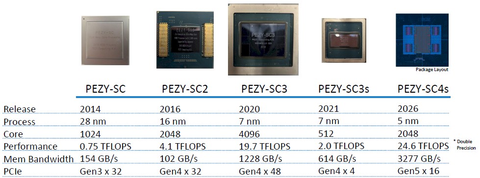
Naoya Hatta, a hardware engineer at Pezy Computing, presented the latest in a line of number-crunching accelerators that have been delivered since the Pezy-1 chip was launched in April 2012 after two years of development. Here is the table Hatta presented at Hot Chips 2025:
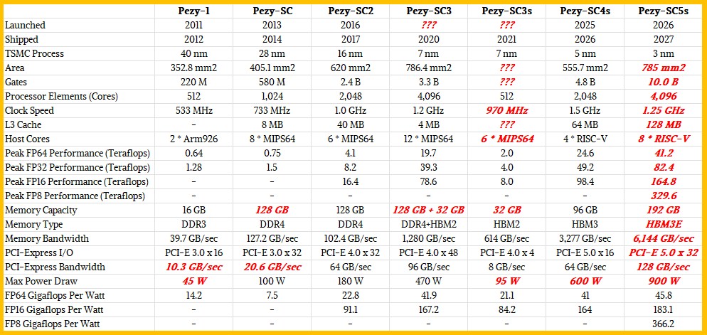
And here is an expanded table with more features and analysis by us:
That Pezy-1 chip, which is not shown in Hatta’s table above, had 512 RISC cores for calculations and image processing and two baby Arm cores, all etched in 40 nanometer processes from Taiwan Semiconductor Manufacturing Co. It ran at 533 MHz and was rated at 266 gigaflops (in floating point format) at double precision and 533 gigaflops at single precision.
In 2013, the SC family – short for Super Computer – accelerators debuted, and were used in a number of supercomputers in 2014 that made their way onto the Top500 and Green500 supercomputer rankings. With the first SC variant, the RISC cores were given simultaneous multithreading with eight threads per core, which meant its 1,024 cores running at 733 MHz could present a total of 8,192 threads to applications. This chip, etched with TSMC 28 nanometer process, could drive 750 gigaflops at FP64 and 1.5 teraflops at FP32 precision. The RISC cores that do calculations are called processor elements, or PEs, have 2 KB caches – two per PE for instructions and one per PE for data, and that aggregates out to 2 MB of L2 instruction and 1 MB of L2 data cache across those cores. Each PE also has a 16 KB scratchpad memory, which aggregates out to 16 MB across the chip.
In the Pezy-SC designs, PEs are organized into blocks of four called “villages,” and four villages are aggregated into “cities” that have shared L2 data and instruction caches, and sixteen cities (or 256 PEs) are aggregated into “prefectures” that have 2 MB of shared L3 cache in the center of each prefecture. The Pezy-SC had four DDR4 memory channels and two PCI-Express 3.0 x8 ports, and had a peak power draw of 100 watts.
With the Pezy-SC2 design that came to market in 2017, the L3 cache was shared across the whole complex and weighed in at 40 MB, significantly helping performance. FP16 half precision math was also added to the RISC cores that comprise the PEs, twice as many PEs were added to the complex, and clock speeds rose by 36.4 percent to 1 GHz. The combined effects of this drove floating point throughput in FP64 and FP32 formats up by 5.5X.
In 2020, with the Pezy-SC3, the PE count was doubled again, clock speeds went up by 20 percent to 1.2 GHz, HBM2 memory was added to the chip complex, and this all boosted floating point throughput by 4.8X. In 2021, a cut-down version of the SC3, called the SC3s, came out, which had only 512 cores and which was created possibly to test the idea of creating smaller chips with only HBM2 memory and ganging them all up to lower the cost of the server nodes based on the Pezy floating point engines. (Not much was said about the SC3s chip.)
With the Pezy-SC4s that was unveiled at Hot Chips last week and that will ship in ExaScaler systems next year, Pezy Computing is dropping down to TSMC 5 nanometer processes and pushing the core count back up to 2,048 and the clock speeds up to 1.5 GHz.
The SC4s chip will also have 96 GB of HBM3 memory with 3.2 TB/sec of bandwidth. Based on the specs in the table we have built above, this chip will have 29.3 percent less area but cram 4.8 billion gates on a device, which is an increase of 45.5 percent over the Pezy-SC3 chip. There is also a 25 percent increase in clock speed, but the clock speed and substantially increased L3 cache, at 64 MB, drives the power dram up to 600 watts, we estimate. That is a 27.7 percent increase in watts against a 24.9 percent increase in floating point throughput, which all seem like fair trades to us. The SC4s also adds support for BF16 processing as well as the FP64, FP32, and FP16 processing supported in the SC3 and SC3s chips.
The Pezy Computing designs are elegant, as we will show in some charts below, and have included some beefy MIPS cores in the past and now RISC-V cores in the SC4s chip that mean a host X86 processor from Intel or AMD is no longer needed to run a Linux operating system to run host software and manage the calculations on the PEs. The accelerators are self-contained, just like the Sparc and Arm processors used in the K and Fugaku supercomputers at RIKEN lab in Japan, the country’s flagship HPC center.
With that, let’s take a look at the SC4s chip complex, and then contemplate what the future SC5s might look like and why Japan is even bothering with all of this. (There are good reasons.)
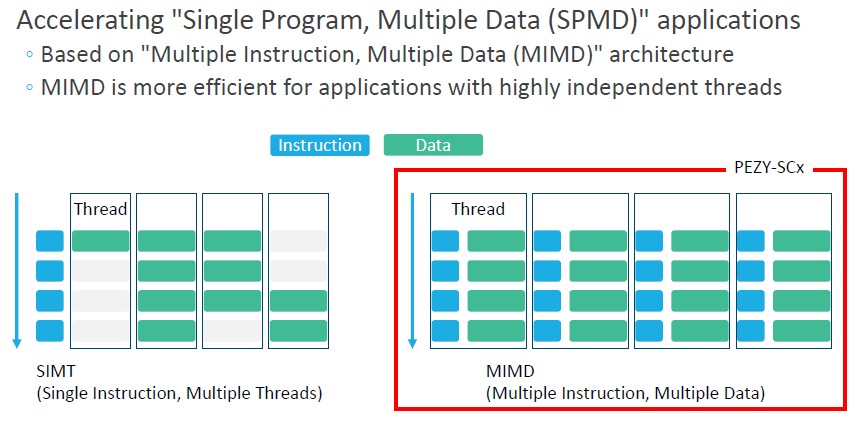
The Pezy Computing architecture is based on a variant of the Multiple Instruction, Multiple Data (MIMD) architecture called Single Program, Multiple Data (SPMD):
To put it into plain American, MIMD is real parallel programming with the most flexibility when it comes to determining the nature of that parallelism. SIMT, such as that used in programming within a GPU or multiple GPUs in a shared memory pool, organizes threads to run operations in parallel on different data in lockstep, thereby increasing efficiency but cutting down on flexibility.
With the SPMD approach used by Pezy Computing and its fine-grained multithreading, threads and data are explicitly scheduled by the program, and therefore you do not need branch predictors and out of order instruction issuing to try to boost parallelism and computational efficiency. That means the cores are simpler and therefore you can cram more of them onto a given piece of silicon. Threads are paired up such that one can take over processing when another one stalls as it is awaiting data from memory, which allows it to hide that latency. (But arguably nothing like a GPU with tens of thousands of cores can do.)
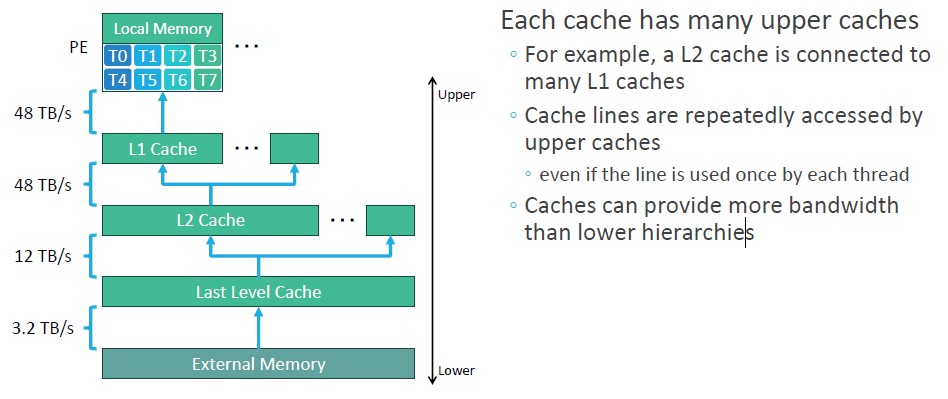
The Pezy architecture has both fine-grained and coarse-grained multithreading, across eight threads per PE, and strives for more balance between compute, memory capacity, and memory bandwidth within and across those PEs. The cache hierarchy is one of the secret sauces to keep those PEs busy:
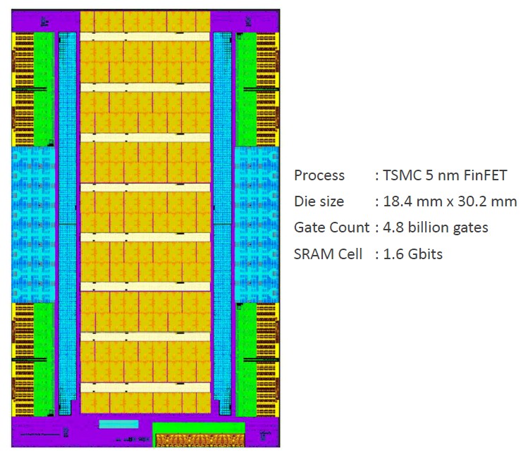
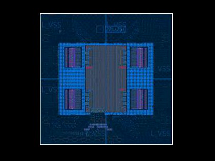
With that, let’s take a look at the Pezy-SC4s chip that debuted at Hot Chips:
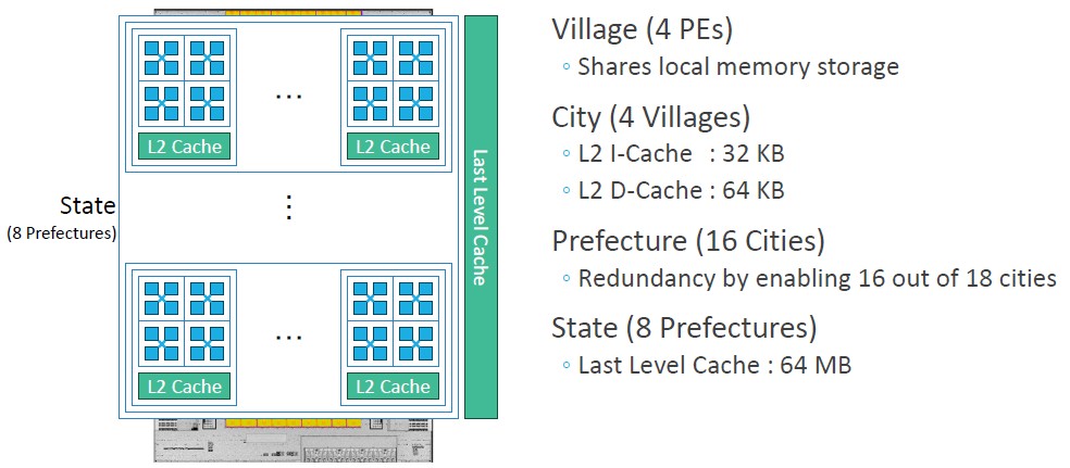
The 2,048 PEs in the design in the block diagram above are shown in yellow, and they can bring 16,384 threads to bear. The PEs in the SC4s chip have 4 KB of L1 instruction cache, 4 KB of L1 data cache, and 24 KB of scratchpad cache, and that is a lot skinnier than in past designs. The PEs are organized in this manner:
As with prior Pezy Computing chips, four PEs are connected into a village that allows them to share their scratchpad caches. A city is comprised of four villages that share 32 KB of L2 instruction cache and 64 KB of L2 data cache. Eighteen cities are linked into a prefecture, and only sixteen are activated to increase the 5 nanometer process yield. And eight prefectures are linked into a state that has a shared 64 MB L3 cache.
Why do we now talk about states? Well, because we think the Pezy-SC5s chip will have two chiplets (or states) in a single socket after a shrink to 3 nanometer processes from TSMC. (So that makes a socket a country?)
These PEs and their caches are interlinked with a custom crossbar bus that has 12 TB/sec of aggregate bandwidth for read operations and 6 TB/sec for write operations.
Anyway, down at the bottom of the chip, so small you can barely see the rectangle, is an IP block that has four “Rocket” open source RISC-V CPU cores running at 1.5 GHz that do in-order scalar processing and that run the Linux host operating system for each SC4s accelerator. Next to the RISC V cores there is also a PCI-Express 5.0 controller with sixteen I/O lanes with 64 GB/sec of bandwidth.
It looks like there is an X86 host back in the mix. The reason might be the ubiquity of AI and HPC software for the X86 platform compared to the RISC-V cores embedded on the SC4s.
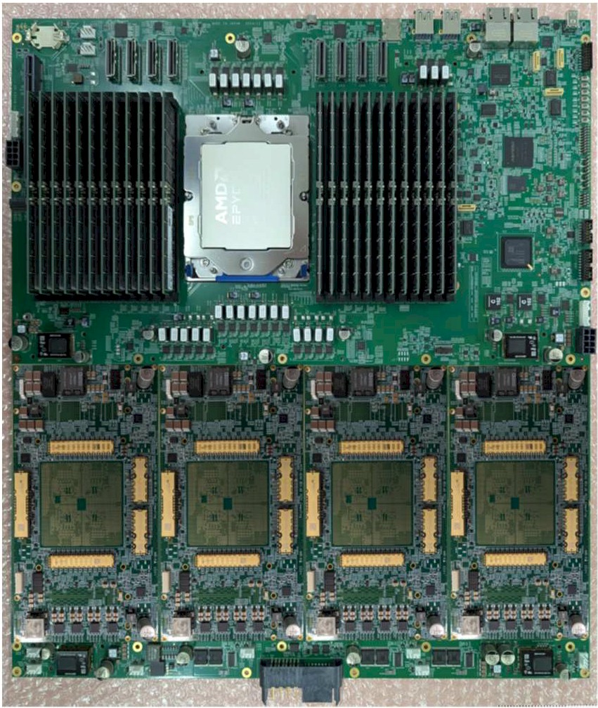
Here is the current system board that Pezy Computing has created for the SC4s accelerator:
There is a 64-core “Turin” Epyc 9555P processor from AMD for the host, plus a 400 Gb/sec NDR InfiniBand controller on the top of the card, with four SC4s accelerators at the bottom and linked to the host over PCI-Express lanes and presumably with PCI-Express switches. Pezy Computing says that it is planning to make a test system with 90 of these nodes, with a total of 737,280 PEs and a peak FP64 performance of 8.6 petaflops.
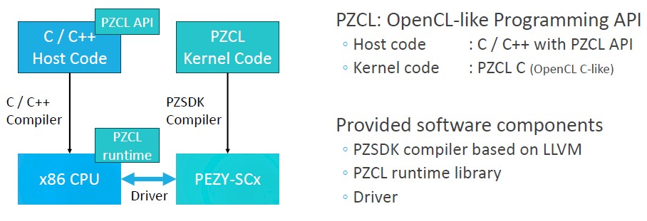
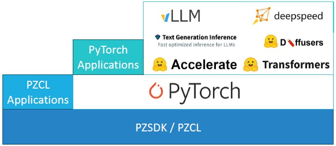
Pezy Computing has had to create its own software stack, of course. And here is what it looks like:
Here is AI stack for the Pezy Computing platform as well:
We have been saying for years that running the PyTorch framework was going to be good enough for a lot of AI work, and it looks like Pezy Computing agrees with this. (We were admittedly more hopeful about the Meta Platforms Llama models, but not as hopeful as Mark Zuckerberg and his AI team turned out to be. . . . Don’t count Zuck out just yet, though.) This far, the Google Gemma3 and Meta Llama3 models have been ported to the SC4s, as has Alibaba Qwen2, Stable Diffusion 2, and Hugging Face HuBert.
We would like to see more real world performance on the SC4s when it ships next year. Hatta said in his presentation that doing genomics analysis using GATK – short for Genome Analysis Toolkit – a quad of Pezy-SC3 chips drove 33 minutes per sample compared to 37 minutes per sample for eight “Hopper” H100 GPUs from Nvidia. That means each SC3 had 2.25X the performance of an H100. The SC4s has about 25 percent more floating point oomph than the SC3, so we conjecture that the SC4s has about 2.8X better performance on GATK. It is not clear how much GATK depends on FP64, but the H100 is far better at FP64 than the “Blackwell” B100 and B300 GPUs from Nvidia.
What HPC centers and AI model builders care about in the end is flops per watt. As you can see from our table above, Pezy Computing has made progress in driving up flops per watt, but it looks like it is going to be trying to hold this metric to minor growth as it crams more compute into sockets. The SC3 delivered 41.9 gigaflops per watt at FP64 precision, and the SC4s looks like it will come in around 41 gigaflops per watt. If the SC5s looks like we expect – basically, a two chiplet version of the SC4s with FP8 math added – it will come in at around 45.8 gigaflops per watt for FP64 math. (It would not be hard to extend that crossbar interconnect across two chiplets.)
The Hopper H200 is 47.9 gigaflops per watt at FP64 (33.5 teraflops divided by 700 watts), and the Blackwell B200 is rated at 33.3 gigaflops per watt (40 teraflops divided by 1,200 watts). The Blackwell B300 has FP64 severely deprecated at 1.25 teraflops and burns 1,400 watts, which is 0.89 gigaflops per watt. (The B300 is really aimed at low precision AI inference.)
Clearly, Pezy can stand toe-to-toe with Nvidia GPUs on flops per watt at high precision and offer more flexible programming for non-AI workloads. Admittedly, the tensor cores in GPUs can crank through twice as much floating point work at FP64 and FP32 precision and also offer much lower precision for AI training (FP8) and inference (FP4).
But the Japanese government can keep Pezy Computing as a hedge and keep a skillset in designing math accelerators in the country by funding this effort. And we think this is exactly why there will be a Pezy-SC5s and even follow-ons. Because you never know when you won’t be able to get a GPU because demand is too high or exports are restricted.
We are fully aware that most of the floating point oomph in the future FugakuNext system going into RIKEN in 2029 is coming from a future Nvidia GPU. But we still think there is plenty of time – and money – to include more than a few racks of Pezy accelerators, too. Why not?
Featuring highlights, analysis, and stories from the week directly from us to your inbox with nothing in between.
Subscribe now
Related Articles

