
Here, we construct an electronic double-layer structure consisting of a pristine bilayer graphene (BLG) at the bottom and a BLG moiré superlattice layer on top, with a hBN layer acting as an insulating spacer, as schematically shown in Fig. 1a. The moiré superlattice is formed between the top BLG layer and the adjacent hBN layer. For simplicity, the pristine BLG and the BLG moiré superlattice will be referred to as “G” and “MG”, respectively. The entire structure is further encapsulated by two additional hBN layers and etched into a Hall bar electrode geometry after assembly on a SiO2/Si substrate (Fig. 1b, see Methods for fabrication details). In such a device, the carrier polarity and density of the two graphene layers can be conveniently adjusted via the inter-layer gate voltage (Vint) and the back gate voltage (VBG).
Fig. 1: Drag device and intra-layer transport.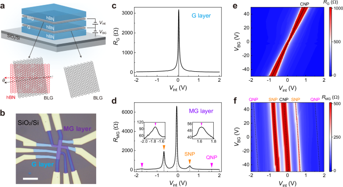
a Schematic of the electronic double-layer structure composed of two bilayer graphene (BLG) layers. The top and bottom BLG layers are separated by a hBN layer with a thickness of ~4.2 nm. The stacking of the top BLG and the hBN spacer forms a moiré superlattice (“MG” layer), while the bottom one is a pristine BLG layer (“G” layer). b Optical image of the drag device assembled on a SiO2/Si substrate. The scale bar is 10 μm. c, d Resistances of the G layer (RG) and the MG layer (RMG) as functions of inter-layer gate voltage (Vint), respectively. The back gate voltage (VBG) was set to 0 V during the measurements. Newly-generated secondary neutrality points (SNPs) and quaternary neutrality points (QNPs) for the MG layer are indicated in (d). Insets in d: zoom-in view of the curves near the QNPs. e, f RG and RMG as functions of Vint and VBG, respectively. The charge neutrality lines of the G/MG layers are indicated by the black solid/dashed lines in (e, f). All these measurements were conducted at T = 1.5 K.
We first examine the intra-layer transport performance. Figure 1c, d presents the Vint-dependent resistances of the G layer (RG) and the MG layer (RMG), respectively. The G layer exhibits slight hole-doping, with the charge neutrality point (CNP) located at Vint = 0.04 V. For the MG layer, typical moiré tuning features are observed (Fig. 1d). In addition to the main CNP at VCNP = −0.05 V, two satellite resistance peaks manifest symmetrically on both the hole and electron sides of the CNP (at Vint = −0.67 and 0.57 V). These peaks correspond to the emergence of secondary neutrality points (SNPs) that arise from the folded superlattice miniband induced by the periodic moiré potential3,4,5,14. We note that the G layer also exhibits two side resistance peaks around its CNP, with significantly reduced amplitude (as detailed in Supplementary Note 1). These minor peaks likely originate from unintentionally formed localized moiré patterns between the G layer and the adjacent hBN layer, and do not affect our subsequent experimental observations.
After extracting the capacitance value of the hBN spacer from the Hall data, the moiré wavelength for the MG layer is estimated to be λ ~ 14.7 nm (as detailed in Supplementary Note 2), indicating a nearly zero mismatch angle between the top BLG and the hBN lattice1,3,15. Additionally, at higher doping levels, a series of resistance peaks known as the quaternary neutrality points (QNPs) are observed based on the corresponding values of Vint16 (as indicated in Fig. 1d). We further obtained the intra-layer resistance mapped as a function of Vint and VBG. Typical results measured at 1.5 K are plotted in Fig. 1e, f, showing resistance peak lines corresponding to both the primary CNP and the newly-generated neutrality points. For the bottom G layer (Fig. 1e), its carrier density and polarity can be readily modulated by either Vint or VBG. The tuning capability of these gates, which is determined by the capacitances of the corresponding dielectric layers (hBN and SiO2), is reflected in the slope of its CNP line. In contrast, for the top MG layer (Fig. 1f), VBG exhibits limited tuning effectiveness due to screening by the G layer. Specifically, applying VBG with Vint fixed fails to shift the Fermi level across moiré-induced SNPs. This is also the reason why the subsequent magneto-drag data were acquired by sweeping Vint rather than VBG (see Supplementary Note 3 for more details).
Inter-layer drag measurements were then conducted by applying a DC current Idrive to the bottom G layer and measuring the resultant drag voltage Vdrag in the top MG layer (see the inset of Fig. 2e). Figure 2a displays the drag resistance \({R}_{{{{\rm{D}}}}}^{{{{\rm{MG}}}}}\) mapped as a function of Vint and VBG measured at 200 K, where moiré-induced features are negligible in the intra-layer transport of the MG layer. Four distinct regions are clearly observed: electron-electron (e-e), electron-hole (e-h), hole-electron (h-e), and hole-hole (h-h). \({R}_{{{{\rm{D}}}}}^{{{{\rm{MG}}}}}\) is negative (positive) when the carrier polarities of two layers are the same (opposite), and is zero along the neutrality point lines of the two BLG layers, aligning with the momentum transfer mechanism17,18,19. These features are identical to those observed in the drag response between two pristine BLG20,21, indicating a negligible moiré tuning effect.
Fig. 2: Moiré drag effect when the MG layer serves as the drag layer.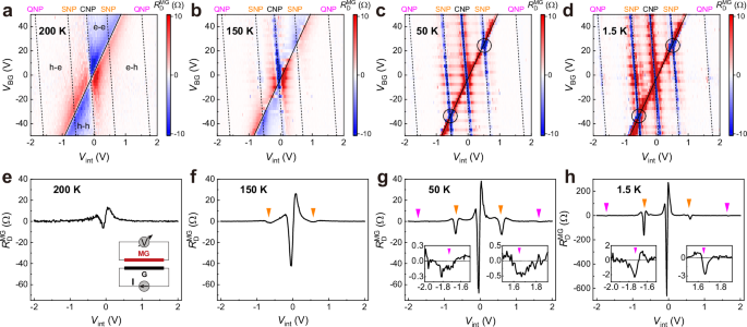
a–d Drag resistance \({R}_{{{{\rm{D}}}}}^{{{{\rm{MG}}}}}\) as a function of Vint and VBG measured at four different temperatures: 200, 150, 50, and 1.5 K. The black solid/dashed lines in (a–d) depict the charge neutrality lines of the G/MG layers. The black circles in (c, d) mark the two cross points between the two SNPs of the MG layer and the CNP of the G layer. e–h \({R}_{{{{\rm{D}}}}}^{{{{\rm{MG}}}}}\) as a function of Vint for VBG = 0 V measured at four different temperatures. Inset in e: schematic of the drag setup. The arrows in (f–h) indicate the locations of SNPs and QNPs of the MG layer. Insets in (g, h): zoom-in views of \({R}_{{{{\rm{D}}}}}^{{{{\rm{MG}}}}}\) vs. Vint curves near the QNPs.
As the temperature decreases, the influence of the moiré potential on the inter-layer transport process becomes pronounced, as evidenced by the emergence and continuous increase of the drag signal along the two SNP and QNP lines of the MG layer (see Fig. 2b–d). It is clear that at temperatures below 150 K, the drag results reflect the intra-layer properties, where the resistance peaks corresponding to the newly-generated neutrality points become evident (see Supplementary Fig. 4). A further comparison of the mapping data shown in Fig. 2a–d reveals a dramatic suppression of the four-region characteristic as the temperature drops. Notably, at 150 K, a striking negative \({R}_{{{{\rm{D}}}}}^{{{{\rm{MG}}}}}\) is evident along the CNP line of the MG layer. This negative signal gets stronger as the temperature decreases, indicating the breakdown of the momentum transfer mechanism17,18,19,20. Similar negative signals are also observed along the SNP and QNP lines. The \({R}_{{{{\rm{D}}}}}^{{{{\rm{MG}}}}}\) vs. Vint curves plotted in Fig. 2e–h provide further insight into the evolution of these negative drag phenomena. At 1.5 K, the \({R}_{{{{\rm{D}}}}}^{{{{\rm{MG}}}}}\) amplitude exceeds 665 Ohms in the vicinity of the CNP (see Fig. 2h), which is significantly higher than the maximum value of 18 Ohms obtained at 200 K (see Fig. 2a). We note that there are striped features parallel to the horizontal axis in Fig. 2b–d, which originate from measurement artifacts detailed in Supplementary Note 4.
A negative drag signal along the CNP line of the drag layer has been observed in experiments involving two pristine BLG layers22, with the emergence temperature typically below 10 K. This phenomenon has been ascribed to the energy transfer mechanism, i.e., inter-layer thermoelectric coupling originating from the spatial thermal gradients due to charge density inhomogeneity23. The observation of negative rather than positive drag indicates that strain rather than charged impurities plays a dominant role in enhancing charge inhomogeneity near the charge neutrality points22,23,24. By further analyzing the dependencies of the drag resistance Rdrag and the partial derivatives of the Peltier coefficient -∂Q/∂μ on the chemical potential μ of the constituent layers, it was found that the drag resistance is strongly related to the Peltier coefficient of the drag layer rather than the drive layer (as detailed in Supplementary Note 5 and Supplementary Fig. 7). This result consists well with the characteristics of energy transfer, indicating that such a thermoelectric mechanism is also applicable to the observed negative drag in our case. The noticeably higher emergence temperature up to 150 K could be attributed to stronger charge density inhomogeneity in the MG layer, a consequence of the moiré-enhanced strain23. In such a superlattice, the variability in stacking configuration between carbon atoms and B-N atoms (i.e., AA, AB, and BA) is divided by domain walls, where the strain accumulates25,26,27. Additionally, there are hot spots of negative drag around the two cross points between the SNPs of the MG layer and CNP of the G layer (as marked by the circles in Fig. 2c, d), which are likely related to the dual-gate-induced band gap opening28,29 (see Supplementary Note 5 and Supplementary Fig. 8).
The observations presented in Fig. 2 demonstrate the significant influence of moiré tuning on the characteristics of inter-layer transport. However, these modulations primarily stem from the direct influence of moiré potential within the MG layer, wherein the drag voltage is collected. Regarding the pristine G layer, the moiré tuning effect is absent when directly measuring its intra-layer transport (left panel of Fig. 3a), even at low temperatures (Fig. 1c, e). This is reasonable, since the influence of the moiré potential is usually restricted to the interface of the moiré superlattice11,12. To further verify this assertion, theoretical calculations of the graphene/hBN moiré potential Vmoiré are performed (see Fig. 3b and Supplementary Note 6 for calculation details). As shown in Fig. 3c, the amplitude of the moiré potential shows a clear exponential decrease with increasing distance z from the graphene-hBN interface, e.g., decreasing by an order of magnitude for each increment in z of 0.21 nm, which is significantly smaller than the thickness of the hBN spacer (~4.2 nm).
Fig. 3: Moiré drag effect when the pristine G layer serves as the drag layer.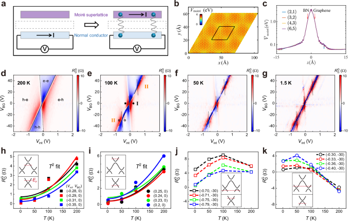
a Schematic diagram of two different configurations for investigating possible moiré tuning effect in an electronic double-layer structure comprising a moiré superlattice and a normal conductor. The left panel illustrates conventional proximity tuning, while the right panel shows long-range tuning facilitated by inter-layer drag interaction. b Planar distribution of the moiré potential Vmoiré in a graphene/hBN moiré superlattice, where the primitive vector of the superlattice is \({{{{\bf{L}}}}}_{1}=m{{{{\bf{a}}}}}_{1}+n{{{{\bf{a}}}}}_{2}\). Here, \({{{{\bf{a}}}}}_{1}\) and \({{{{\bf{a}}}}}_{2}\) are the lattice vectors of graphene, and (m, n) = (6, 5). c Dependency of moiré potential strength on the out-of-plane distance (z) from the graphene-hBN interface for superlattices with (m, n) = (2, 1), (3, 2), (4, 3), and (6, 5). The red arrows indicate the planes of the hBN and graphene layers. d–g Drag resistance \({R}_{{{{\rm{D}}}}}^{{{{\rm{G}}}}}\) as a function of Vint and VBG measured at four different temperatures: 200, 100, 50, and 1.5 K. The black solid/dashed lines indicate the charge neutrality lines of the G/MG layers. h, i Temperature-dependent \({R}_{{{{\rm{D}}}}}^{{{{\rm{G}}}}}\) for typical sites in Region “I” (as indicated in e) and corresponding quadratic fitting results. j, k Temperature-dependent \({R}_{{{{\rm{D}}}}}^{{{{\rm{G}}}}}\) for typical sites in the newly-generated Region “II” at negative Vint (as also indicated in e). Insets in h–k: schematics of the band structures and the positions of the Fermi level for the MG layer (top) and the pristine G layer (bottom).
What will happen if we switch between the drive layer and drag layer, by applying the drive current within the MG layer and collecting the drag voltage in the pristine G layer (as schematically illustrated in the right panel of Fig. 3a)? Given that inter-layer drag is a coupled effect of intra-layer transport and inter-layer interaction mainly dominated by Coulomb scattering, it is possible to achieve long-rang moiré tuning effect on the pristine G layer from the distant MG layer.
The correspondingly measured drag resistance \({R}_{{{{\rm{D}}}}}^{{{{\rm{G}}}}}\) at 200 K is shown in Fig. 3d as a function of Vint and VBG. The four-distinct-region feature is centered by the double CNPs, and the overall magnitude of drag resistance is identical to the case when the MG layer acts as the drag layer (see Fig. 2a), indicating the validity of the Onsager reciprocity relation at this elevated temperature (see Supplementary Fig. 11b, 12b). Upon lowering the temperature to 100 K (Fig. 3e), a similar four-distinct-region feature emerges in the regions surrounding the cross points between the CNP line of the G layer and the two SNP lines of the MG layer (Region “II”). Such behaviors become more pronounced at 50 K (see Fig. 3f), wherein a distinct self-similar drag spectrum is observed. These characteristics, which appear around the moiré-generated neutrality points, clearly demonstrate the impact of the moiré tuning on the carrier transport of the pristine G layer. As mentioned earlier, the thickness of the insulating spacer between the two conducting layers is significantly greater than the decay length of the static moiré potential. The substantial extension of moiré influence here leverages the long-range nature of drag interactions, a dynamic process involving inter-layer momentum/energy transfer mediated by Coulomb scatterings.
From the mapping data obtained at an even lower temperature of 1.5 K (see Fig. 3g), these moiré tuning features become less significant. Notably, a negative \({R}_{{{{\rm{D}}}}}^{{{{\rm{G}}}}}\) along the CNP of the G layer becomes dominant, which can also be attributed to a thermoelectric origin of energy transfer22, similar to the case where the MG layer serves as the drag layer (as detailed in Supplementary Note 5). However, detailed features are completely different when comparing Fig. 3g with Fig. 2d, indicating a breakdown in the Onsager reciprocity relation at low temperatures (see Supplementary Note 7). Such low-temperature non-reciprocity has also been observed in another device (see Supplementary Fig. 13), indicating its reproducibility.
To quantitatively depict the evolutionary behavior of the drag response, in Fig. 3h–k we further plot the temperature-dependent \({R}_{{{{\rm{D}}}}}^{{{{\rm{G}}}}}\) curves for several sites in different regions (as indicated in Fig. 3e). These sites are chosen away from the CNP of the G layer to minimize the impact of anomalous negative drag. For the sites in Region I, \({R}_{{{{\rm{D}}}}}^{{{{\rm{G}}}}}\) exhibits a well-defined T2 dependence (see Fig. 3h, i), aligning with the momentum transfer mechanism in the Fermi liquid regime17,18,19,20,30. On the other hand, a non-monotonic temperature dependence is observed for the sites in Region II, as typically shown in Fig. 3j, k (see Supplementary Fig. 14 for the data of more sites). This phenomenon can be attributed to the competition between the inter-layer drag interaction and the moiré tuning effect. As the temperature decreases, the inter-layer drag interaction dominated by Coulomb scattering is suppressed by the decreased scattering phase space13,31, while the moiré potential effect intensifies simultaneously. Notably, the sign of \({R}_{{{{\rm{D}}}}}^{{{{\rm{G}}}}}\) in the e-h region changes when the temperature decreases to 100 K (see Fig. 3k). This is due to the transition of carrier type in the MG layer from hole to electron (see Supplementary Fig. 4d), which also results from the moiré-induced superlattice miniband.
As for the magneto-transport within the moiré superlattice, a fractal energy spectrum known as Hofstadter’s butterfly has been observed due to moiré potential tuning3,4,5. Figure 4a, b shows the intra-layer resistance RG and RMG as functions of Vint and magnetic field B at T = 1.5 K, respectively. The pristine G layer exhibits a standard Landau fan diagram, with minima in RG occurring at filling factors v = ±4 N (where N is an integer Landau level index)32,33,34, as indicated by the gray lines in Fig. 4c. In contrast, the MG layer displays a typical Hofstadter’s butterfly spectrum (see Fig. 4b). By comparing the corresponding Wannier diagram presented in Fig. 4d, the Landau levels (LLs) developed from the CNP at n = 0 are clearly seen. However, LLs fanning out from the two SNPs at n = ±4n0 exhibit reduced intensity due to spectral overlap with dominant CNP features (Supplementary Fig. 15), consistent with previous studies on graphene/hBN moiré superlattices3,4,15.
Fig. 4: Hofstadter’s butterfly spectrum of magneto-drag resistance.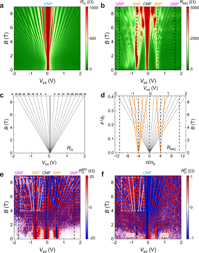
a, b Intra-layer resistance RG and RMG as functions of Vint and magnetic field B, respectively. The black solid/dashed lines indicate the charge neutrality lines of the G/MG layers. c Schematic Landau fan diagram of the bottom G layer according to the experimental data shown in (a). The gray lines label the filling factor v of the LLs. d Schematic Landau fan diagram of the top MG layer, replotted in terms of the dimensionless parameter n/n0 and ϕ/ϕ0. Here, ϕ = B⋅A is the flux per moiré unit area A at magnetic field B, and ϕ0 = h/e is a flux quantum. h is Planck’s constant, e is the elementary charge, n is the carrier density, and n0 = 1/A corresponds to one electron filling per moiré unit cell area A. The gray and orange lines indicate three sets of LLs developed from the CNP and the two SNPs according to the experimental data shown in (b), which can be expressed using the Diophantine equation of (n/n0) = v(ϕ/ϕ0) + s. Here, ν denotes the filling factor of LL, and s represents the intercept of the gap trajectory, which is 0 for the main CNP and ±4 for SNPs. e, f Inter-layer drag resistance \({R}_{{{{\rm{D}}}}}^{{{{\rm{MG}}}}}\) and \({R}_{{{{\rm{D}}}}}^{{{{\rm{G}}}}}\) as functions of Vint and B, respectively. The black solid/dashed lines indicate the charge neutrality lines of the G/MG layers. The white dashed box outlines the high-field regime where the moiré-modulated features are evident, and the white solid lines indicate the corresponding LLs developed from the hole-side SNP of the MG layer. All measurements were conducted at T = 1.5 K and VBG = 0 V.
Below, we investigate how the moiré potential affects the magneto-drag response for the two different drag configurations. Figure 4e shows the mapping of \({R}_{{{{\rm{D}}}}}^{{{{\rm{MG}}}}}\) with respect to (Vint, B), with the MG layer serving as the drag layer. In the low-field regime, significant negative drag signals emerge around both the CNP and the two SNPs of the MG layer (see also Supplementary Fig. 16a). This moiré-modulated negative drag signal intensifies with increasing B35,36,37, which could be attributed to the enlarged scattering phase space37,38. Upon further increasing the field into the quantized field regime, e.g., above 1.5 T, a rather complex spectrum of \({R}_{{{{\rm{D}}}}}^{{{{\rm{MG}}}}}\) unfolds. \({R}_{{{{\rm{D}}}}}^{{{{\rm{MG}}}}}\) develops clear oscillations with frequent sign reversals (see also Supplementary Fig. 16b). As detailed in Supplementary Note 8, these oscillations are closely correlated with the LL fillings in the drag MG layer, including the ones developed from CNP and also moiré-induced SNPs.
Remarkably, the drag mapping of \({R}_{{{{\rm{D}}}}}^{{{{\rm{G}}}}}\) (see Fig. 4f) also distinctly shows the influence of moiré tuning in the low-field regime (<1.5 T) with the pristine G layer serving as the drag layer. Clear drag signals arise around the two SNP lines of the MG layer (see also the Hall data presented in Supplementary Fig. 18). These findings further highlight the extension of moiré tuning across the hBN spacer (Supplementary Note 9 for more details). Even under high fields, it is observed that the Landau fan diagram fanning out from the CNP of the drag G layer is disturbed by the LLs arising from the SNPs of the MG layer. For the regime corresponding to the hole-side SNP (as marked by the white dashed box), the presence of external positive drag induces a marked deviation in the \({R}_{{{{\rm{D}}}}}^{{{{\rm{G}}}}}\) spectrum from the standard profile characterized by alternating positive and negative signals. In contrast, the modulation effect is less pronounced in the regime corresponding to the electron-side SNP. Such electron-hole asymmetry is consistent with the intra-layer transport of the MG layer (see Fig. 1d, f, 4b), where the moiré-tuning effect is also more pronounced on the hole side. Previous studies have demonstrated that this characteristic is common in hBN/graphene moiré superlattices and is relevant to asymmetries in the on-site energy within the hBN layer and the next-nearest-neighbor inter-layer coupling between graphene and hBN1,15.
Therefore, the observed moiré-modified magneto-drag mappings can be ascribed to an inter-layer version of Hofstadter’s butterfly spectrum. Analogous to the zero-field case, the violation of Onsager reciprocity relation when switching between the drive and drag layers (see Fig. 4e, f) is highly relevant to the different action mechanisms of the moiré potential: direct tuning within the drag layer when the MG layer serves as the drag layer, versus remote tuning through inter-layer drag interaction when the pristine G layer serves as the drag layer. However, the magneto-drag spectra are more intricate compared to the intra-layer ones (see Fig. 4a, b). In addition to amplitude oscillations, the sign of drag resistance also varies with the LL filling of the drag layer (Fig. 4e, f). As detailed in Supplementary Note 10 and Supplementary Fig. 20, 21, the drag signal transitions from negative to positive as the Fermi level moves from below to above the half-filling of the LLs. This corresponds to a change in carrier type in the drag layer, from electron-like to hole-like behaviors, between adjacent filling factors39.
In summary, our study has demonstrated that the influence range of moiré tuning can be greatly extended from the moiré superlattice interface to a distant conductor, leveraging the long-range nature of drag interaction. This innovative approach, i.e., constructing an electronic double-layer structure incorporating a moiré superlattice, holds promise for broad applicability in systems with rich moiré physics, such as twisted bilayer graphene7,8 and transition-metal chalcogenide moiré structures9,40. On the other hand, the pristine graphene layer could also be extended to numerous 2D conductors, particularly those where moiré lattice formation is impractical or generates undesirable periodicities. Furthermore, the extension of the impact range for other potentials generated by structural modulation, such as artificial periodic potential in patterned dielectric superlattices41, could be investigated.
Note added
During the submission of this manuscript, we became aware of a related but independently developed study that performed drag measurements in a similar structure comprising a graphene/hBN moiré superlattice42. The zero-field results of the two studies are consistent with each other.