
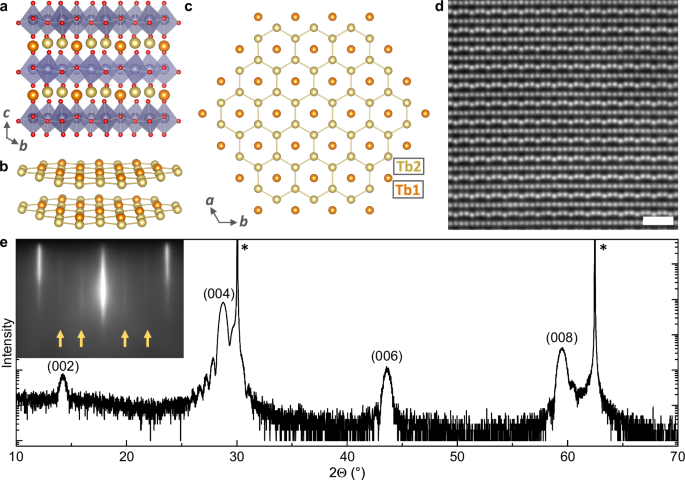
Thin-film growth
Among the group of quantum spin liquid candidate materials, TbInO3 lends itself particularly well to epitaxial thin-film realization: it is well lattice matched to commercially available substrates and belongs to a larger family of isostructural functional hexagonal oxides enabling further epitaxial engineering and integration into oxide electronic heterostructures20. Here, we use reactive oxide molecular-beam epitaxy (MBE) to synthesize ultrathin epitaxial films of TbInO3 on (111)-oriented yttria-stabilized zirconia (YSZ) substrates. The growth was optimized with respect to the Tb/In stoichiometry using in situ reflection high-energy electron diffraction (RHEED), see Supplementary Fig. S1, and confirmed with ex situ X-ray diffraction (XRD) and scanning transmission electron microscopy (STEM). A narrow growth window is identified for phase-pure TbInO3 films (Supplementary Figs. S1 and S2)21. The (\(\sqrt{3}\times \sqrt{3}\)) R30° reconstruction seen in the RHEED pattern of stoichiometric TbInO3 is indicative of the lattice trimerization, which serves as the primary order parameter of the improper ferroelectricity. This lattice trimerization is observed directly at the growth temperature and confirms a high ferroelectric TC exceeding our growth temperature of 860 °C. Figure 1e shows a θ–2θ XRD scan, which confirms the purely (001)-oriented layered hexagonal structure. Laue oscillations around the (004) reflection of TbInO3 are testament to sharp film interfaces, as further confirmed by a low surface roughness determined by atomic-force microscopy (Supplementary Fig. S1). The in-plane lattice mismatch between bulk TbInO3(0001) and a 30° rotation of YSZ(111) is −0.8%. In-plane X-ray reciprocal space mapping (RSM) reveals that the films gradually relax with respect to the substrate lattice with increasing thickness (Supplementary Fig. S3). While at a thickness of 8 nm, the film lattice is fully aligned with the substrate, the 15 nm and 29 nm films show gradual relaxation. Likewise, local strain maps based on STEM images show that the 8 nm film has a uniform ϵxx across the interface (Supplementary Fig. S4). In the 15 nm film, except for a region of increased ϵxx near the film-substrate interface, there is a slight negative ϵxx within the film (Supplementary Fig. S5), which reveals partial relaxation of the in-plane strain, as expected from the X-ray RSM data.
We use STEM to visualize the atomic structure of the film (Fig. 1d and Supplementary Fig. S6). As shown in the high-angle annular dark field STEM (HAADF-STEM) image in Fig. 1d, the film is highly crystalline and ordered, composed of alternating layers of terbium and indium atoms. This layered structure confines the spins on the terbium sublattice to 2-D planes, providing a frustrated environment9.
The terbium sublattice further displays the up-up-down displacement pattern, which is a consequence of the trimerization of the lattice structure (Fig. 2a). This lattice distortion drives the ferroelectric order in hexagonal indates, just as in hexagonal manganites14,15 and ferrites22. By fitting the corrugation of the terbium lattice, both the amplitude and phase of the order parameter can be spatially resolved23. The trimerization mapping shown in Fig. 2b–d reveals a multi-domain state with a preference of up-polarized domains at the film-substrate interface, interspersed with down-polarized domains that tend to widen towards the top surface of the film. This is in contrast to the preferably single-domain state found in both hexagonal manganites and ferrites grown on the same type of YSZ substrate24,25. A similar nanometer-scale multi-domain state is realized in YMnO3 thin films on platinum-coated Al2O3 substrates26,27. The TbInO3 thin films display all six trimerization domains (Fig. 2b–d and Supplementary Figs. S7 and S8) with a smaller domain size and thus larger number of domain walls in comparison to the bulk crystals of TbInO310. A thinner 8 nm TbInO3 also shows a similar domain pattern (Supplementary Fig. S7). It has been proposed that the domain walls could host magnetic edge states or novel spin excitations10, making the TbInO3 thin films with rich domain structure23 an exciting platform to study these emergent properties.
Fig. 2: Improper ferroelectric domain mapping in a 15 nm TbInO3 epitaxial thin film.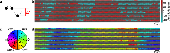
a The up-up-down trimerization of the terbium sublattice fit to a sinusoid to extract the distortion amplitude (Δ) and phase. b A map of the local distortion amplitude in a 15 nm TbInO3 thin film overlaid on a HAADF-STEM micrograph. c The trimerization phase corresponds to six possible ferroelectric domains. d A map of the improper ferroelectric domains in the same region as (b), based on the color scale given in (c).
We extract the average Tb1–Tb2 displacement amplitude (Fig. 2a) to be 34.8 pm, which is slightly less than the value of ~ 40 pm reported for bulk crystals10. Using density functional theory (DFT), we estimate the magnitude of the spontaneous polarization in our films, given a 35 pm Tb1–Tb2 displacement, to be 7.11 μC cm−2 (See Supplementary Note I). The thinner sample shows a slightly smaller displacement (Supplementary Fig. S8), possibly due to strain or interface clamping imparted from the substrate. While the displacement in the thicker film corresponds to a polarization similar to the reported value of the ferroelectric polarization of the hexagonal manganites and ferrites, our estimated polarization is larger than the electrical polarization measured in bulk TbInO310 at 77 K, despite our slightly smaller distortion.
Frustrated rare-earth magnetism
Having established the growth of high-quality epitaxial thin films, we next investigate the low-temperature magnetic properties of our TbInO3 films. Bulk crystal TbInO3 has been suggested to host a quantum spin liquid ground state characterized by persistent spin fluctuations down to at least 0.1 K in the absence of long-range magnetic order9,10. It remains unclear, however, how such a state transfers to the thin-film limit. Here, we use a combination of conventional and scanning SQUID magnetometry to gain insight into the nature of the magnetic ground state of our epitaxial films.
Firstly, we note that the YSZ substrates used here, even though intrinsically diamagnetic, are found to exhibit a weak paramagnetic response, due to trace amounts of magnetic impurities. Hence, low-temperature measurements, where such paramagnetic substrate contributions become larger, are particularly challenging given the small magnetic volume of the thin film. We account for this parasitic magnetic signal by measuring both the magnetic signal of the total film + substrate system as well as the substrate signal alone, as further described in “Methods” and Supplementary Note II. We also confirm that the origin of our extracted thin-film magnetic signal is from the terbium sublattice of the TbInO3 film by performing X-ray magnetic circular dichroism (XMCD) at the Tb M4,5 edge. This element-specific measurement is not susceptible to background from the substrate paramagnetism and yields data with an excellent agreement with our SQUID magnetometry measurements (Supplementary Fig. S9).
The TbInO3 film contribution to the DC magnetic susceptibility between 1.8 K and 300 K is shown in Fig. 3a. We find that there is no ordering or spin freezing down to 1.8 K, as evidenced by the lack of splitting between field-cooled (FC) and zero-field-cooled (ZFC) curves (additional ZFC-FC curves at lower applied fields are shown in Supplementary Fig. S10). Note that the Néel temperature of possible magnetic impurities occurs from 2.4 K (Tb2O3) to 7.85 K (Tb4O7)28 but is not detected in our measurements. Fitting the inverse susceptibility according to the Curie–Weiss law, we extract an effective Tb3+ moment μeff of 10 μB, which is, within the error of our experiment, consistent with the free ion value of 9.7 μB. We further extract a Curie–Weiss temperature θCW = −11 K, which is similar to, albeit somewhat lower than, that measured in bulk crystals9,10 and indicates frustrated antiferromagnetic interactions. By comparing the magnetic susceptibility using applied magnetic fields along the in-plane and out-of-plane directions of the film, an XY easy-plane anisotropy is identified at temperatures above 23 K, whereas the anisotropy is strongly reduced below this temperature (Supplementary Fig. S11). Such a temperature-dependent change of magnetic anisotropy was also seen in bulk TbInO3 at a similar cross-over temperature9,10.
Fig. 3: SQUID magnetometry on a 38 nm film of TbInO3 on YSZ(111).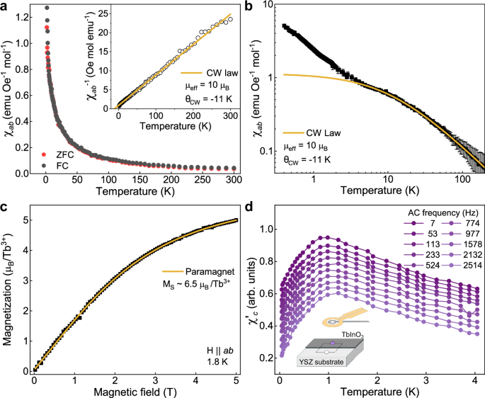
a In-plane magnetic susceptibility measured using an applied field of 1000 Oe as a function of temperature upon warming after field-cooling (black) and zero-field cooling (red). No splitting of the two curves, as would be indicative of magnetic ordering, is observed down to 1.8 K. A linear Curie–Weiss fit to the inverse susceptibility yields a Curie–Weiss temperature of −11 K and an effective Tb3+ moment μeff of approx. 10 μB. b Magnetic susceptibility extended further down to 0.4 K, using a field of 2000 Oe, similarly reveals no long-range order. A deviation from the high-temperature Curie–Weiss behavior is evident below 5 K. The error bars represent the measurement uncertainty as provided by the instrument (see “Methods”). c In-plane magnetic field dependence of magnetization yields a saturation magnetization MS of ca. 6.5 μB/Tb3+ at 1.8 K. d AC magnetic susceptibility along the out-of-plane c-axis of the film, collected between 44 mK and 4 K by scanning SQUID magnetometry, displays a sharp downturn below 1 K. A background contribution from the substrate has been characterized on an area where the film had been removed (see schematic in inset) and subtracted from the data. The y-axis corresponds to the 7 Hz dataset (in emu mol−1), all other curves have been offset for clarity.
Further evaluating the in-plane magnetic susceptibility down to as low as 400 mK (Fig. 3b), we find no evidence of long-range magnetic order in our films, although a deviation from the high-temperature Curie–Weiss behavior is observed below 5 K. The temperature dependence of the susceptibility in this low-temperature regime corresponds to a lowered effective magnetic moment accompanied with a smaller frustration index, and is likely related to the depopulation of exited electronic states on the terbium sites. Indeed, in bulk samples, a similar behavior is observed below 7.5 K. Based on the isothermal field dependence of magnetization at 15 and 1.8 K, we extrapolate saturation moments of ca. 7.4 and 6.7 μB/Tb3+ ion, showing a gradual decrease with decreasing temperature (Supplementary Fig. S12). Models of the depopulation of thermally populated crystal electric field levels in other rare-earth based frustrated magnetic oxides show a similar gradual reduction in saturation moment29. In previous studies on bulk TbInO3, it has been suggested that the depopulation of the first excited crystal electric field (CEF) level on the Tb1 site (located at around 0.65 meV) leads to a singlet ground state with a much reduced or vanishing magnetic moment9 and an effective magnetic lattice below 5 K with stuffed honeycomb geometry (Fig. 1c). Although our estimated saturation moment of ca. 6.5 μB/Tb3+ at 1.8 K (Fig. 3c) could be consistent with the stuffed honeycomb model considering a suppressed Tb1 moment9, our data do not permit determining the exact magnetic configuration of Tb1 and Tb2 in our films. We also note that other studies of TbInO3 bulk crystals using Raman spectroscopy30 and inelastic neutron scattering11, have suggested a triangular magnetic lattice with similar magnetic ground state for both Tb1 and Tb2 sites.
We next assess the AC susceptibility of the TbInO3 film, using scanning SQUID microscopy, in the same regime below 5 K where the higher energy CEF levels are depopulated and TbInO3 likely exists in its magnetic ground state. To characterize the substrate contributions to the thin-film susceptibility, we ion-mill etch away part of the film, exposing the bare substrate underneath (see “Methods” and Supplementary Note III for details). We use a scanning SQUID microscope in a dilution refrigerator to locally measure, with micrometer-scale spatial resolution, side-by-side the susceptibility of the bare substrate and film + substrate together. The probe field is generated by an excitation coil concentric with the SQUID’s sensitive area, which applies a local field of approximately 500 μT along the c-axis of the sample. This approach therefore probes the out-of-plane susceptibility of the sample. In the weak screening limit, the susceptibility of the film is found by subtracting the bare substrate susceptibility from the susceptibility measured from the film + substrate. This allows us to determine the magnetic susceptibility specific to the TbInO3 film down to 44 mK, an order of magnitude lower in temperature than previous work9.
Figure 3d shows the AC susceptibility measured with the field along the c-axis of TbInO3 from 44 mK to 4 K. At higher temperatures, the AC and DC susceptibilities exhibit similar behavior. However, in the AC susceptibility, a maximum is observed around 1 K, below which the susceptibility decreases. In addition, the temperature at which the maximum susceptibility occurs weakly depends on the applied AC frequency. The AC susceptibility appears spatially uniform within our spatial resolution.
A downturn in the AC magnetic susceptibility is observed in various magnetic systems—including spin glasses, two-dimensional spin liquid candidates, superparamagnets, systems that magnetically order and combinations of these. In each system, different mechanisms are at play to cause a downturn in the AC susceptibility31,32,33,34,35. Our frequency dependence is reminiscent of that reported for spin freezing in spin glasses, in which disorder and geometric frustration hinder long-range order31 (see Supplementary Note IV for an analysis of the frequency dependence). In spin glasses, the downturn occurs at a temperature at which the relaxation rates fall below the excitation frequency.
Our in-plane DC susceptibility shows paramagnetic behavior down to at least 400 mK (Fig. 3b) without a turnover as seen in the AC susceptibility. Generally, a turnover in DC susceptibility would occur at a lower temperature than in AC measurements. Extrapolating our frequency dependence using models for spin freezing transitions (see Supplementary Note IV), a turnover in DC would be expected around 600 mK. However, the DC and AC susceptibility measurements probe along different crystallographic directions in this anisotropic system raising the possibility that spin fluctuations are not freezing in the in-plane directions. In addition, the applied probe field in the DC measurements is substantially larger than the AC field, which may result in a temperature shift of a turnover in the in-plane DC susceptibility36,37.
Unconventional transport in Pt/TbInO3 heterostructures
With the epitaxial stabilization of TbInO3 thin films, we are poised to measure non-local transport in these materials. As shown in Fig. 4a, we construct devices with a measurement geometry that has been used to demonstrate magnon spin transport in insulating ferromagnets, such as yttrium iron garnet38, and more recently antiferromagnets39. This setup allows for the detection of voltages generated from charge-spin interactions between the platinum layers and the TbInO3 film, namely the spin Hall effect (injector to film) and inverse spin Hall effect (film to detector). In addition, by tracking the detector voltage readout at both positive (\({V}_{\det }^{+}\)) and negative (\({V}_{\det }^{-}\)) injection currents, the signal can be separated into a symmetric term (\({V}_{{{{\rm{det,sym}}}}}={V}_{\det }^{+}-{V}_{\det }^{-}\)) that excludes heat-related effects but preserves direct transport, such as magnon transport, and an asymmetric term (\({V}_{{{{\rm{det,asym}}}}}={V}_{\det }^{+}+{V}_{\det }^{-}\)) that includes heat-related effects, such as spin Seebeck effect39,40. While TbInO3 lacks the ordered moment to form magnons, exotic carrier physics was revealed by THz conductivity in bulk TbInO3 crystals18. Interestingly, this phenomena persists at temperatures well above the Curie–Weiss temperature, which traditionally defines the spin liquid regime. We thus probe the non-local transport of the TbInO3 samples to determine whether these carriers can be manipulated electrically.
Figure 4b shows Iinj–Vdet,sym curves collected at temperatures between 200 K and 400 K from a device with a channel separation of 400 nm. The response grows above room temperature, indicating the apparent activation of a high-temperature transport mechanism. This signal can have a few different contributions, each with different current dependencies: a spin Hall effect contribution, which scales linearly with I (V ∝ I), and thermal contributions due to Joule heating, which scale quadratically with I (V ∝ I2). We perform fits of the form V = R1I + R2I2 to extract coefficients corresponding to linear and quadratic components of the signal. These fits are plotted as solid lines in Fig. 4b, and the temperature dependence of the R1 coefficients is shown in Fig. 4c. We see the onset of this linear scaling coefficient above 300 K, potentially indicative of high-temperature spin transport in the TbInO3 film. No magnetic field dependence (in-plane or out-of-plane) was observed at any temperature using field sweeps up to 9 T (Supplementary Fig. S13). A control measurement was conducted by applying voltage across the detector and injector to measure DC current across the spacing shown in Supplementary Fig. S14. A temperature-dependent cross current was observed, with a negligibly small magnitude and a cross resistance exceeding 1 GΩ.
Fig. 4: Non-local transport signatures in TbInO3 devices.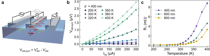
a Schematic of the device, consisting of parallel platinum strips on a TbInO3 film. b Symmetric voltage signal measured as a function of injector current amplitude at temperatures ranging from 200 K to 400 K. Solid lines represent quadratic fits of the form V = R1I + R2I2. Error bars show the standard deviation of four measurements. c Linear fit coefficient R1 versus temperature for devices with spacing values d = 400, 600, and 800 nm. Error bars represent the least squares standard deviation fit error.