
The topology of the GHMSIW attenuator is shown in Fig. 1. The attenuator is simulated by the finite element simulation tool, Ansys High Frequency Structure (HFSS) version 2024. The proposed GHMSIW attenuator operates at the wideband of 5.5 GHz to 8.5 GHz. The GHMSIW attenuator comprises of a simple half mode SIW transmission line with a gap of 8 mm×0.5 mm at the center of the line. The gap for graphene deposition is 1 mm×0.3 mm according to the desired aspect ratio. There is a biasing pad close to the gap of the graphene. The graphene pad is appropriately positioned to increase attenuation in the transmission coefficient. The electric field intensity is higher at the open end of the HMSIW line.
Fig. 1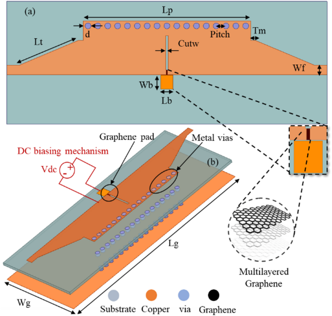
The schematic of the proposed GHMSIW attenuator (a) Top view (b) 3D view with a DC biasing mechanism for measurements.
The higher resistance of graphene blocks the signal transmission, while the lower resistance allows the maximum transmission. SIW based circuits21 are also used to derive dielectric permittivity along with other conventional methods22. The various design parameters of SIW can be taken from the sensor as in21. The cutoff frequency (fc10), effective width (weff), diameter (d) of vias, and the distance between the center of the via (pitch) are calculated by using (1) and (2). Graphene is modeled as a lumped resistive element with assigned resistance values ranging from 138 Ω/□ to 1302 Ω/□ based on the measured graphene impedance characterization values found in literature13 and23.
$$\:{\text{f}}_{\text{c10}}=\frac{1}{2\text{W}\sqrt{\mu\:\epsilon\:}}$$
(1)
$$\:\text{W}\text{siw}=\text{W}+\frac{{d}^{2}}{0.95\text{P}}$$
(2)
Where W, fc10, and P represent the effective width, cutoff frequency, and pitch between the centers of the adjacent vias, respectively. The effective W and patch length Lp determine the lower and upper cutoff frequencies of the SIW. The values of d and P are optimized to minimize the radiation losses. The dimensions of the proposed attenuator in Fig. 1 are Lp, Lt, Wf, d, Pitch, Wb, Lb, Lg, Wg, Tm, and cutw: 34 mm, 12 mm, 1.94 mm, 0.6 mm, 2 mm, 2.5 mm, 2.5 mm, 65 mm, 25 mm, 0.5 mm, and 1 mm, respectively.
Fig. 2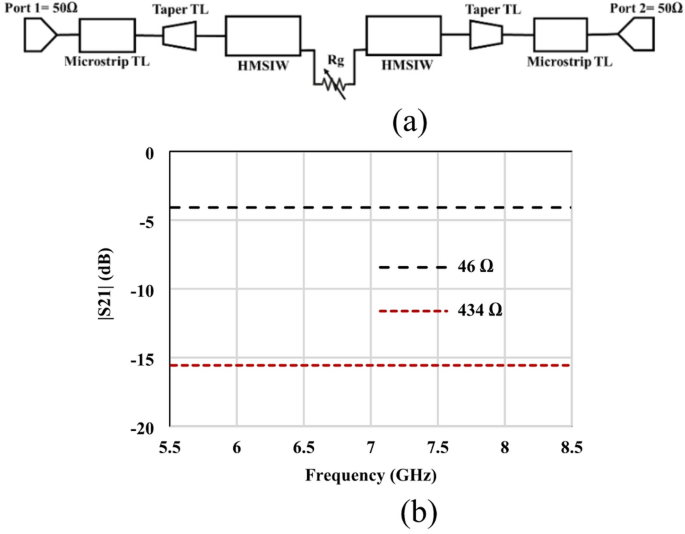
Equivalent circuit model of the GHMSIW attenuator (a) Circuit model (b) simulated amplitude of the transmission coefficient (S21).
The equivalent circuit model of the proposed HMSIW attenuator is depicted in Fig. 2 (a). The graphene variable resistance Rg is connected in the center between the two HMISW lines. The circuit model consists of two 50 Ω input ports, a microstrip, tapered, and a half-mode SIW transmission line. The resistance of graphene in the equivalent circuit is Rg. The conversion of lumped resistance (Ω) to sheet resistance (Ω/□) values is related to each other through the aspect ratio of the deposited graphene (1 mm x 0.3 mm). The gap size in the direction of current flow is 0.3 mm, so the minimum measured resistance is 46 Ω, and the maximum is 434 Ω (Fig. 2b), with corresponding minimum and maximum sheet resistance values of 138 Ω/□ and 1302 Ω/□, respectively.
A plot of the S21 is shown in Fig. 3. It is clear that in the absence of graphene, the transmission coefficient is less than − 15dB throughout the entire frequency band. This means that negligible amount of power is transmitted between the two ports, and the majority is attenuated. Thus, it is clear from the empty gap analysis that the gap is large enough to provide negligible transmission. In other words, the parasitic capacitance is negligible according to (3) as in24.
$$\:\text{C}=\frac{\text{A}.{\upepsilon\:}}{\text{d}}$$
(3)
where ε is the relative permittivity of the dielectric, A is the overlapping area, and d is the distance between traces.
Fig. 3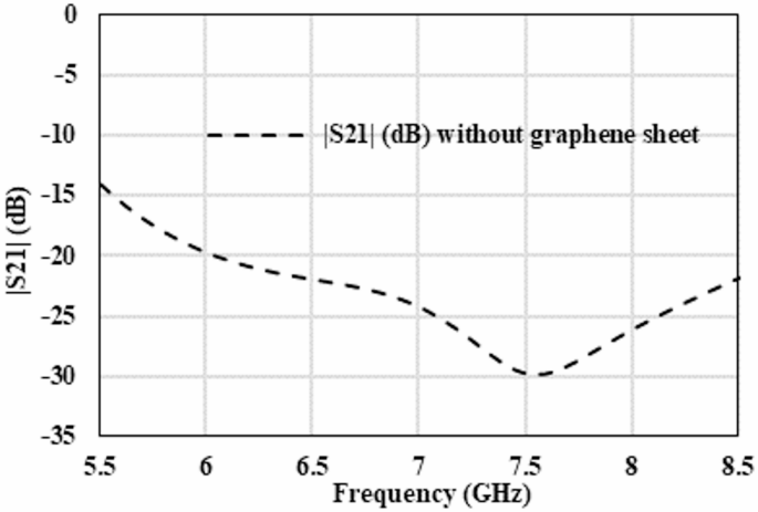
Simulated amplitude of S21 of the attenuator without graphene.
The electric field distribution of the GHMSIW attenuator is depicted in Fig. 4. The transmission of the signal between the ports can be qualitatively characterized from the electric field distribution. The electric field distribution of GHMSIW shows an increased transmission between port 1 and port 2 for low graphene resistance values (Fig. 4 (a)). For higher resistance of graphene, the signal transmission from port 1 to port 2 is reduced (Fig. 4(b)). This shows that the attenuation can be effectively tuned by changing the resistance values of graphene.
Fig. 4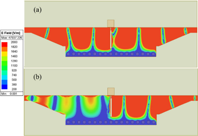
Surface currents distribution of GHMSIW attenuator at 7 GHz with two graphene pads. The graphene surface impedance is (a) Rg = 138 Ω/□ and (b) Rg 1302 Ω/□.
The topology of the GHMSIW phase shifter is shown in Fig. 5. The proposed GHMSIW phase shifter operates in the frequency band of 6.5 to 9.5 GHz with a center frequency of 8 GHz. The GHMSIW phase shifter consists of a half mode SIW transmission line, connected to a full-mode SIW stub through graphene pads. The full mode SIW stub helps in introducing additional phase variation in the transmission coefficient when the resistance of the graphene pads is lowered.
Fig. 5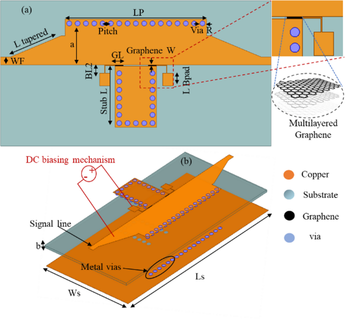
A schematic of the proposed GHMSIW phase shifter (a) Top view (b) 3D view.
To maximize the flow of the transmitting signal into the stub and the resultant phase variation, the full-mode SIW stub is positioned at the open side of the half-mode SIW transmission line. The cutoff frequencies of a waveguide can be calculated according to the dimensions given in (4) and (5) as in19.
$$\:{\text{f}}_{\text{c,\:}\text{mn}}=\frac{\text{c}}{2\sqrt{{\epsilon\:}_{r}\:}}\sqrt{({\raisebox{1ex}{$m$}\!\left/\:\!\raisebox{-1ex}{$a$}\right.)}^{2}+({\raisebox{1ex}{$n$}\!\left/\:\!\raisebox{-1ex}{$b$}\right.)}^{2}\:}$$
(4)
$$\:{\text{f}}_{\text{c,\:m0}}=\frac{\text{m}\text{c}}{2\text{a}\sqrt{{\epsilon\:}_{r}\:}}$$
(5)
Where, m, n are the integers, and b represents the height of the SIW between the top and bottom layers, fc, mn are the cutoff frequencies. The effective width (a) determine the lower (6.5 GHz) and upper (9.5 GHz) cutoff frequencies of the TE10 and TE20 modes of the waveguide. The values of via diameter (d) and pitch (P) are optimized to minimize the radiation losses. The dimensions of the proposed phase shifter in Fig. 5 are Lp, Ltapered, Wf, ViaR, Pitch, BL1, BL2, LBpad Ls, Ws, GL, a, b and Lstub: 34 mm, 12 mm, 1.94 mm, 0.6 mm, 2 mm, 2.5 mm, 94 mm, 3 mm, 65 mm, 30 mm, 10 mm, 0.813 mm, 0.3 mm, 10 mm, respectively.
Fig. 6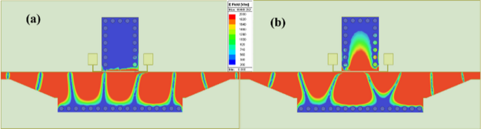
E-filed distribution of GHMSIW phase shifter at 8 GHz with two graphene pads. The graphene surface impedance is (a) Rg = 600 Ω/□ and (b) Rg = 60 Ω/□.
Fig. 7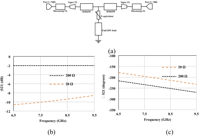
Circuit model analysis of the GHMSIW phase shifter (a) Equivalent circuit model (b) S21 amplitude (c) S21 phase.
Figure 6 shows the E-field distribution of the proposed phase shifter for different graphene resistance values. For the higher graphene sheet resistance value (Rg = 600 Ω), the GHMSIW phase shifter shows an unperturbed transmission between port 1 and port 2 (see Fig. 6 (a)). The higher resistance of graphene makes this phase shifter a simple half-mode SIW-based transmission line. In the case of lower resistance of the graphene sheet (Rg = 60 Ω), there is an increased phase shift in the transmission of the signal. It is obvious from the E-field distribution that the path for the signal changes and the electrical length of the transmission line increases, causing a delay in the transmission of the signal. For lowered graphene sheet resistance values, the signal passes through the SIW stub, as shown in Fig. 6 (b).
The equivalent circuit model of the proposed HMSIW phase shifter is depicted in Fig. 7 (a). The circuit model consists of two 50Ω input ports, a microstrip, tapered, half-mode SIW transmission line and a stub. The equivalent resistance of the two graphene pads is Req = R1||R2. The simulated amplitude and phase of S21 of the equivalent circuit, which includes 200Ω and 20 Ω graphene resistance, is taken from the sheet resistance adjusted according to the aspect ratio23, is shown in Fig. 7 (b) and (c). The lumped resistance (Ω) value is measured first and then converted to sheet resistance (Ω/□) by the aspect ratio of the deposited graphene (1 mm x 0.3 mm). The gap size in the direction of current flow is 0.3 mm, so the measured resistance values 200Ω and 20Ω (Fig. 7b and c) correspond to sheet resistance 600Ω∕□ and 60Ω∕□, respectively.