
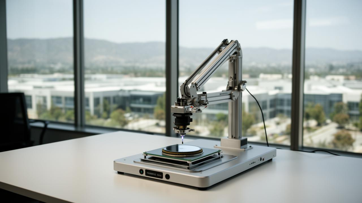
Hanmi Semiconductor is establishing a 100% subsidiary, “Hanmi USA,” in San Jose, California. The company is investing $1.5 million (approximately 2 billion won) with the goal of an official launch in the fourth quarter of this year. The move is a strategic step to respond to the growth of the artificial intelligence (AI) semiconductor market and to diversify a revenue structure that is heavily concentrated on specific clients.
This decision puts into action the US expansion plan announced by Chairman Kwak Dong-shin at the company’s Incheon headquarters last May. The new subsidiary will be responsible for the development and sales of semiconductor manufacturing equipment, related parts, and materials, as well as providing technical support and equipment maintenance (CS) for local customers. A Hanmi Semiconductor official stated, “We will respond to the expansion of semiconductor manufacturing facility investments and increasing equipment demand in the US, and strengthen our local technical support.”
With the addition of the US subsidiary, Hanmi Semiconductor’s overseas bases will increase to five, joining existing locations in Taiwan, China, Vietnam, and Singapore. San Jose was chosen as the base because it is a region densely populated with major semiconductor companies and Outsourced Semiconductor Assembly and Test (OSAT) providers. Key players such as Micron—believed to be its largest customer—along with Intel, NVIDIA, and AMD are located nearby. The location allows the company to provide close support to existing memory customers while simultaneously expanding its sales network to foundry and AI chip companies.
A Revenue Rollercoaster Driven by Customer Concentration
Hanmi Semiconductor’s performance has fluctuated wildly over the past year. Revenue, which was 180 billion won (approximately $127.0 million) in the second quarter of last year, declined for three consecutive quarters to 50.9 billion won (approximately $35.9 million) in the first quarter of this year. However, in the second quarter, revenue skyrocketed to 251.1 billion won (approximately $177.2 million), marking a record high on a quarterly basis. In essence, revenue plunged by more than 70% within a year, only to rebound by 393.3% in a single quarter.
Notably, the company posted an earnings shock in the first quarter of this year despite the steep growth of the HBM market. This was because orders for its flagship TC Bonder equipment were delayed as a major client postponed its HBM4 investment. As a result, TC Bonder revenue in the first quarter plummeted 96.6% year-over-year to just 4 billion won (approximately $2.8 million).
The fundamental cause of this increased performance volatility is cited as the high dependency on specific clients. Last year, the largest customer accounted for 44.0% of revenue, while the second-largest represented 14.8%, meaning just two clients made up 58.8% of total sales. This is a structure where orders from two companies dictate the majority of overall revenue. While it is inevitable in the semiconductor equipment industry for performance to be tied to customer order cycles, the excessive dependency amplified the magnitude of the fluctuations.
Targeting System Semiconductors with an Expanded Equipment Portfolio
Hanmi Semiconductor is also reorganizing its equipment portfolio in line with its customer diversification strategy. Following the launch of the ‘FC Bonder 75’ last year, the company successively introduced the ‘FC Bonder 3.5’ and the ‘2.5D TC Bonder 40’ in June of this year. This expands its product lineup, which was previously focused on HBM TC Bonders for memory, to include 2.5D packaging equipment for AI system semiconductors.
The 2.5D TC Bonder 40 is specialized for chip-on-wafer processes, while the FC Bonder 3.5 and FC Bonder 75 are specialized for connecting wafers and substrates. The strategy is to broaden the customer base beyond existing memory clients to include foundries, OSAT providers, and AI chip companies.
Major Clients’ US Investments Also a Factor
The establishment of production bases in the US by major clients also served as a backdrop for accelerating the subsidiary’s creation. SK Hynix is building an advanced packaging production base and R&D facility for AI memory in Indiana. Micron is constructing a DRAM and High Bandwidth Memory (HBM) manufacturing base in Boise, Idaho, and a large-scale memory production facility in Syracuse, New York. Intel and Amkor Technology are also operating or preparing foundry and advanced packaging facilities in Arizona.
Hanmi Semiconductor’s establishment of a US subsidiary is interpreted as a two-track strategy to provide rapid technical support locally in step with its clients’ expanding US investments, and further, to reduce order volatility by discovering new customers.