
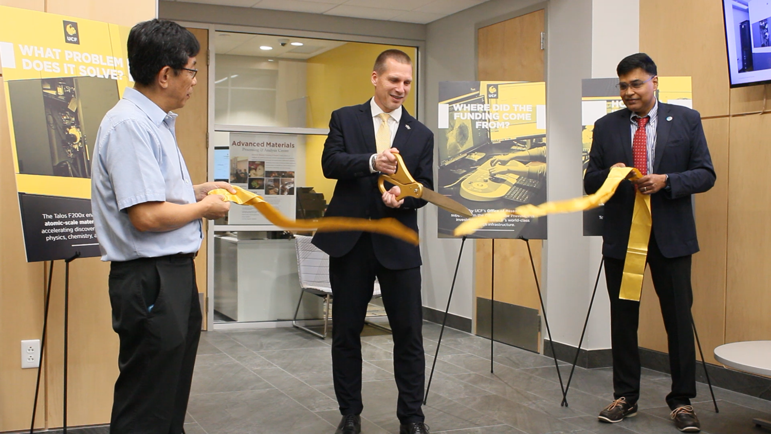

Dr. Jiyu Fang, director of the Advanced Materials Processing and Analysis Center (left); Winston Schoenfeld, vice president for research and innovation at the UCF College of Optics and Photonics (middle); and Dr. Sudipta Seal, chair of the Department of Materials Science and Engineering (right), cut the ribbon for the new High-Resolution Transmission Electron Microscope in the Research 1 building on Tuesday.
Orion Boone
The College of Engineering and Computer Science held a ribbon-cutting ceremony on Tuesday to celebrate its new high-resolution electron microscope, which will bring new research opportunities to students, faculty and researchers. This package aired in the March 4 webcast.
Orion Boone
Attendees filed into a narrow room in the Research 1 building as the College of Engineering and Computer Science held a ribbon-cutting ceremony for the new High-Resolution Transmission Electron Microscope Tuesday.
Engineering faculty provided demonstrations of the instrument, looking at the physical and chemical properties of elements at an atomic level. The night included several rounds of these demonstrations to give all guests a chance to see the microscope in action.
The $4-million tool will give researchers at UCF incredibly precise chemical mapping of even delicate materials, Associate Professor Dr. Akihiro Kushima said.
“There are some similar microscopes [at other Florida universities], but we have the most recent detectors that can detect X-ray signals from the materials more efficiently,” Kushima said. “You can get really fine resolution for elemental mapping, you can see the individual atoms.”
The microscope, a Thermo Fisher Talos F200X, will be incorporated into students’ future coursework and available for researchers, faculty and students to use.
Mikhail Klimov, research engineer at UCF’s Advanced Materials Processing and Analysis Center, explains the inner workings of the High-Resolution Transmission Electron Microscope in the Research 1 building on Tuesday.
Orion Boone
The instrument is housed in UCF’s Materials Characterization Facility at its Advanced Materials Processing and Analysis Center. Its insights into structure-property relationships will drive innovation across multiple sectors, including the semiconductor, biomedical and aerospace industries, Dr. Sudipta Seal, chair of the Department of Materials Science and Engineering, said in a press release.
Paul Sohl is the CEO of the Florida High Tech Corridor, which works with 23 counties and three universities to build the capacity for innovation. He said he was awed at the demonstration given at the ribbon-cutting ceremony and is excited about the research to come from the microscope.
Attendees file into a narrow room to take a close look at atoms in the Research 1 building at the ribbon-cutting ceremony for the new High-Resolution Transmission Electron Microscope on Tuesday.
Orion Boone
“Measuring materials at the micron level, that to me is unfathomable – and that’s where the nanotech world is going,” Sohl said.
UCF already had a similar, simpler microscope, but the HRTEM can see a more complex chemical makeup than the previous one. The new microscope goes beyond a replacement, Winston Schoenfeld, vice president for research and innovation at the UCF College of Optics and Photonics, said.
“This is really about an investment in the people that use it,” Shoenfeld said. “It’s the students. It’s the faculty and researchers.”