
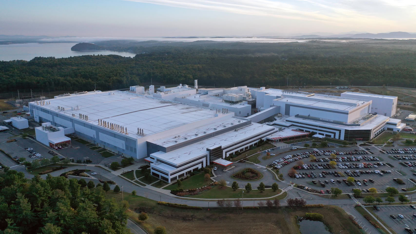
GlobalFoundries announced that it has been selected to provide the technology and to operate two planned semiconductor fabs at its Malta, New York, site. This is not a direct investment from GF but rather came as a new U.S.-Japan initiative involving up to $21 billion in funding. The first 300 mm fab will be funded with an initial investment of around $10 billion. GF expects to break ground later this year, with production planned to begin in 2029. In a second phase, another fab is planned with another $10 billion investment at a later date. When fully operational, each fab will produce around 900,000 wafers annually. GF expects to reach baseline capacity around 2031-2023 for the first fab, and projects 2033 for the second one. The expansion comes as the company seeks new opportunities in advanced packaging and semiconductor manufacturing. In April, AMD announced plans to work with GF on co-packaged optics (CPO) for its next-generation Instinct MI500 AI accelerators, scheduled for 2027. The company is also preparing to bring its 7 nm-class FDX Fusion technology into mass production at its Dresden, Germany, facility in 2028.
Separately, GF has reached an agreement with the U.S. Department of Commerce to amend its CHIPS and Science Act award, reallocating $955 million to accelerate investments in silicon photonics, silicon-germanium (SiGe), and advanced packaging at its facilities in Malta, New York, and Burlington, Vermont. Under a separate agreement, the U.S. government will receive an approximately 4% equity stake. In 2025, GlobalFoundries ranked fifth among the world’s top ten foundries, behind TSMC, Samsung, SMIC, and UMC.