
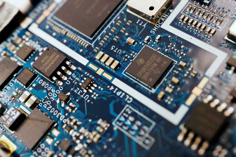
In a high-security laboratory in Shenzhen, China, scientists have developed a prototype machine capable of producing advanced semiconductor chips crucial for technologies such as artificial intelligence and military applications, a goal that the U.S. has long sought to prevent. This prototype, completed in early 2025 and currently in the testing phase, occupies almost an entire factory floor. It was assembled by a group of engineers previously employed by ASML, a Dutch semiconductor company, who reverse-engineered the extreme ultraviolet lithography machines (EUVs) essential for chip production.
EUV machines utilize extreme ultraviolet light to carve out infinitesimal circuits on silicon wafers—an ability that remains predominantly in the hands of Western companies. Despite being operational and successfully generating extreme ultraviolet light, the machine has yet to produce functioning chips. ASML CEO Christophe Fouquet recently suggested that China might require “many, many years” to acquire this technology, but the existence of the prototype indicates that China’s timeline may be significantly shorter than projected.
However, significant technical challenges persist, predominantly in achieving the precision found in Western optical systems. The availability of components from older ASML machines in the secondary market enabled China to construct its domestic prototype, with aspirations to produce working chips by 2028, although more realistic estimates suggest 2030. This is still ahead of the decade that many analysts had anticipated would be required for China to equal the West’s semiconductor capabilities.
The prototype’s development is a culmination of a six-year initiative aimed at semiconductor self-sufficiency—a priority of President Xi Jinping. While China’s semiconductor ambitions have been publicly stated, the Shenzhen EUV project has remained largely secretive. The project is part of a broader strategy overseen by Ding Xuexiang, a close associate of Xi Jinping and head of the Communist Party’s Central Science and Technology Commission.
Huawei plays a crucial role in orchestrating this initiative, coordinating efforts among various companies and research institutes. The operation has been compared to the U.S. Manhattan Project, with the aim of achieving complete self-sufficiency in advanced chip manufacturing.
Historically, ASML stands as the sole enterprise to have perfected EUV technology, with machines priced around $250 million that are pivotal for creating state-of-the-art chips utilized by companies like Nvidia and AMD. ASML’s development of EUV technology spanned nearly two decades and involved extensive investment before its first commercial chips were produced in 2019.
Since 2018, the U.S. has pressured the Netherlands to prohibit ASML from selling EUV equipment to China, and in 2022, the Biden administration broadened export controls to limit China’s access to cutting-edge semiconductor technology. These controls target not just EUV systems but also older deep ultraviolet lithography machines, aimed at keeping China at least one generation behind in chip development. The U.S. State Department has stated that enforcement of these export controls has been strengthened, working with international partners to address potential loopholes.
Chinese semiconductor development has faced hindrances due to these export restrictions, impacting major players like Huawei. Sources emphasize the confidentiality surrounding the Shenzhen project, noting that participants were instructed to use false identities to maintain operational secrecy. Recruited engineers included former ASML employees who possess crucial technical expertise, allowing the team to successfully reverse-engineer the technology.
Recruitment efforts for engineers proficient in semiconductor technology have been aggressive since 2019, with offers of substantial signing bonuses and incentives such as home-buying assistance. Notable recruits include Lin Nan, ASML’s former head of light source technology, who has made strides in patent developments related to EUV light sources.
While ASML claims to safeguard its trade secrets rigorously, it faces challenges due to European privacy laws, making it difficult to monitor former employees. The Dutch intelligence community has warned that China has utilized extensive espionage operations to acquire advanced knowledge and technology from Western nations, further illustrating the competitive landscape. Even with legal frameworks in place, enforcement of confidentiality agreements across international borders remains complex.
Furthermore, the recruitment of personnel working in advanced technology sectors continues to draw scrutiny, as individuals have been reportedly incentivized with excess benefits, including dual citizenship arrangements that allow some to maintain affiliations with multiple nationalities despite official restrictions.
As the Chinese government pushes towards its semiconductor self-sufficiency objectives, it is evident that their efforts to narrow the technological gap with the West are intensifying. Despite the hurdles ahead, the Shenzhen project represents a significant step forward in China’s quest to dominate semiconductor manufacturing, with implications not only for the global technology landscape but also geopolitically regarding supply chains and technological dependencies.
INSIDE CHINA’S EUV FAB
ASML’s latest EUV systems measure the size of a school bus and weigh 180 tons, with China’s prototype significantly larger to enhance power, though it remains crude compared to ASML’s machines. The Chinese model is hampered by challenges in acquiring optical systems from Carl Zeiss AG, a key supplier for ASML. China’s primary research institutes, especially the Changchun Institute of Optics, Fine Mechanics and Physics (CIOMP), are crucial in developing domestic alternatives. CIOMP made strides in integrating extreme-ultraviolet light into the optical system projected to be operational by early 2025, despite needing substantial improvements.
To attract talent, CIOMP advertised “uncapped” salaries for PhD lithography researchers and grants totaling 4 million yuan ($560,000) along with personal subsidies of 1 million yuan ($140,000). Analyst Jeff Koch from SemiAnalysis noted that if China achieves a reliable, powerful light source with minimal contamination, it would signify substantial progress. China’s advantage lies in not starting from scratch since commercial EUV already exists.
To procure necessary components, China is using salvaged parts from older ASML machines and sourcing from ASML suppliers via secondhand markets, often utilizing intermediary companies to obscure the ultimate buyer. Export-restricted components from Japan’s Nikon and Canon are also integrated into the prototype, though Canon indicated no awareness of such reports. Recent auctions regularly listed older semiconductor fabrication equipment, including ASML lithography equipment, indicating a market presence for such parts.
China has a dedicated team of around 100 recent graduates engaged in reverse-engineering both EUV and DUV lithography machine components. Each workspace is monitored via individual cameras to document the disassembly and reassembly process critical for developments in lithography. Workers who successfully reassemble components receive bonuses as an incentive.
Huawei plays a significant role in the entire supply chain, from chip design and fabrication to final product integration, closely monitored by CEO Ren Zhengfei, who briefs high-ranking officials on progress. Employees at Huawei often work in isolation within semiconductor teams, sleeping on-site during workweeks, with strict communication limits imposed to maintain project confidentiality, emphasizing the high security surrounding their work on semiconductor advancements.
With information from Reuters