
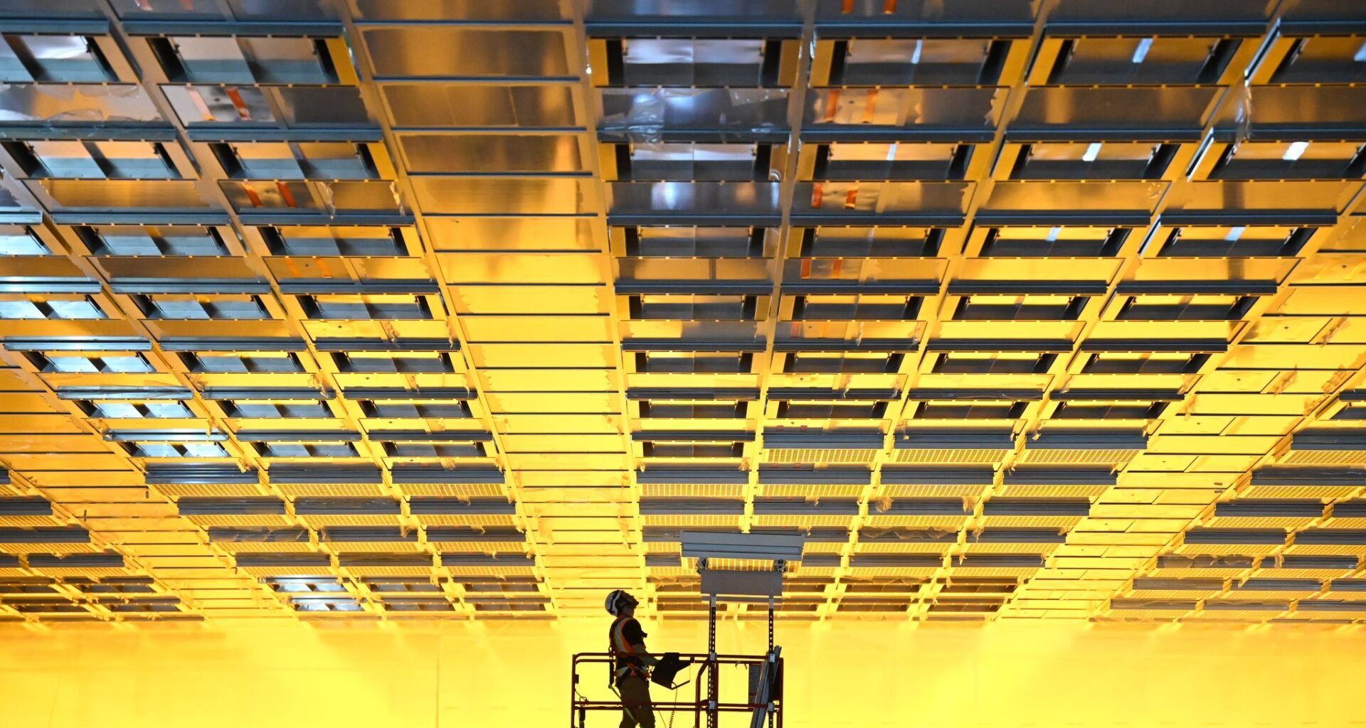
Air filters are installed in a clean room at the new NanoFab Reflection building on Feb. 25 at the Albany NanoTech Complex in Albany. The first machine needed for the building’s new $10 billion chip lithography center is being installed this week.
Will Waldron/Times Union
Gov. Kathy Hochul speaks at a news conference announcing Albany Nanotech’s $10 billion chip research program with Micron and IBM, which will use a new ASML lithography machine in the new NanoFab Reflection building at Albany NanoTech. The High NA Extreme Ultraviolet Lithography Center at NanoFab Reflection is expected to cost $600 million to build.
Lori Van Buren/Times Union
Siding is added to the new NanoFab Reflection building at the Albany NanoTech Complex in Albany. The first machine needed for the building’s new $10 billion chip lithography center is being installed this week.
Will Waldron/Times Union
ALBANY — The new $10 billion computer chip lithography center at Albany NanoTech, the state’s computer chip research and development center on Fuller Road, is taking shape.
Gov. Kathy Hochul’s office announced Thursday that the first manufacturing machine, or “tool,” is being installed in NanoFab Reflection, the new building at Albany NanoTech that will house what’s known as the High NA Extreme Ultraviolet Lithography Center.
Article continues below this ad
The crown jewel of the center will be the world’s most expensive computer chip manufacturing tool, the TWINSCAN EXE: 5200B, a $400 million extreme ultraviolet lithography machine made by the Dutch firm ASML. That tool, which weighs 160 tons, will be delivered in several shipping containers to Albany NanoTech later in the summer.
Extreme ultraviolet lithography has been in use in the chip industry for nearly a decade, but the TWINSCAN EXE: 5200B is a next-generation EUV machine that has a higher aperture, or wider lens, allowing for clearer, better images on the chips.
But last week, a different, yet also important tool, was delivered for installation at NanoFab Reflection, the CLEAN TRACK LITHIUS Pro DICE. The machine, a coater and developer machine that is used early on in the chipmaking process, is made by Tokyo Electron, or TEL. TEL has a research office at Albany NanoTech.
Make the Times Union a Preferred Source on Google to see more of our journalism when you search.
Add Preferred Source
“New York State is leading the nation in semiconductor manufacturing and R&D, and the installation of this tool for the High NA EUV Lithography Center will allow New York to remain at the forefront of chip innovation,” Hochul said in a statement.
Article continues below this ad
High NA EUV lithography is considered vital to being able to make next-generation chips, including those used in artificial intelligence applications. The technology is so important for military and economic uses that the U.S. government has worked with ASML to prohibit it from selling its new machines to China.
The chips race with China led to Congress passing the CHIPS and Science Act, which provided $52 billion in subsidies to chip manufacturers to build new factories in the U.S. The CHIPS and Science Act also spurred the creation of a new federal chip research program, which the new High NA EUV center at Albany NanoTech is part of.
Hochul has made high-tech research and manufacturing a priority for her administration and earmarked $1 billion in state money for the High NA Extreme Ultraviolet Lithography Center. The new building that will house the lithography center, NanoFab Reflection, is expected to cost $600 million to build.
The ASML machine alone can cost up to $400 million. The other members of the center, including TEL, are putting up the remaining $9 billion in equipment and spending needed for the center, which will focus on the lithography stage of chip-making in which the microscopic design for individual chips is “etched” onto a 12-inch silicon wafer.
Article continues below this ad
Today’s chips are only just now being made using High NA EUV machines. NY Creates, the nonprofit that owns Albany NanoTech, was able to get one of the first High NA EUV machines from ASML through its relationship with Micron Technology, the memory chipmaker that is building a manufacturing campus outside of Syracuse. Micron allowed NY Creates to essentially jump the line and buy one of the new machines that it had planned to buy from ASML as it expands in New York and Idaho as part of the CHIPS and Science Act.
That lithography process starts with a special light-sensitive, or photo-resist, coating being applied to the wafer. This is done by the TEL machine, the CLEAN TRACK LITHIUS Pro DICE.
The wafer is then exposed to extreme ultraviolet light in the TWINSCAN EXE: 5200B machine.
The wafers are then returned to the CLEAN TRACK LITHIUS Pro DICE, where a solvent is applied, revealing the chip design.
Article continues below this ad
TEL makes an older version of its coater and developer machine called the LITHIUS Pro Z, which has been in use for a decade in chip factories. The new model is designed to work with extreme ultraviolet lithography and was introduced to the market in December.
TEL donated the new tool to NY Creates as part of the $10 billion lithography program.
“The installation of the LITHIUS Pro DICE system at the Albany NanoTech Complex High NA EUV Lithography Center underscores what is possible when the semiconductor ecosystem comes together with a shared commitment to innovation,” said Alex Oscilowski, president of TEL Technology Center America, TEL’s operation at Albany NanoTech. “As High NA EUV comes online, it will accelerate advances in AI, high-performance computing, and the technologies that will shape how the world connects, computes and creates.”