

Support CleanTechnica’s work through a Substack subscription or on Stripe.
China’s covert effort to build an extreme ultraviolet lithography (EUV) system, described as a Manhattan Project and leveraging Chinese nationals with experience from key Dutch EUV manufacturer ASML, is not interesting because it appeared suddenly or because it surprised intelligence agencies. It is interesting because it exposed how industrial capability actually accumulates over time. EUV lithography sits at the peak of semiconductor manufacturing complexity. It is not one machine, but a tightly coupled system of lasers, plasma physics, precision optics, vacuum systems, control software, materials science, and manufacturing discipline. Reaching even a partial working prototype as China has done requires thousands of deeply trained engineers and years of iterative failure. China’s achievement does not mean it has closed the gap with ASML. It means that the distance is now measured in years, not decades.
Modern advanced chips are defined by how small their features are, measured in nanometers, and that number matters because it determines how many transistors can be packed onto a chip, how fast they can switch, and how much energy they consume. Chips described as 7 nm, 5 nm, 3 nm, and now moving toward 2 nm are not literally built with features of exactly that size, but the labels track successive generations of shrinking transistor dimensions and tighter tolerances. At these scales, older lithography techniques break down. Deep ultraviolet lithography, which uses longer-wavelength light, can no longer reliably pattern the finest features without resorting to multiple exposures, complex workarounds, and rising defect rates. Extreme ultraviolet lithography uses 13.5 nm light, substantially extending achievable resolution and reducing multi-patterning, even as ultimate feature size remains constrained by optics, resist behavior, and process variability.
EUV lithography is exceptionally difficult to implement. Light at 13.5 nm cannot pass through lenses and must instead be reflected by multilayer mirrors manufactured and aligned to near-atomic precision. The EUV light itself is generated by firing high-power lasers at microscopic tin droplets to create plasma. The entire system operates in high vacuum and demands extraordinary control of vibration, temperature, contamination, and timing. Only Dutch manufacturer ASML succeeded, after years of collaboration with specialized suppliers, deep involvement from leading chipmakers, and sustained public and private investment across Europe and the United States.
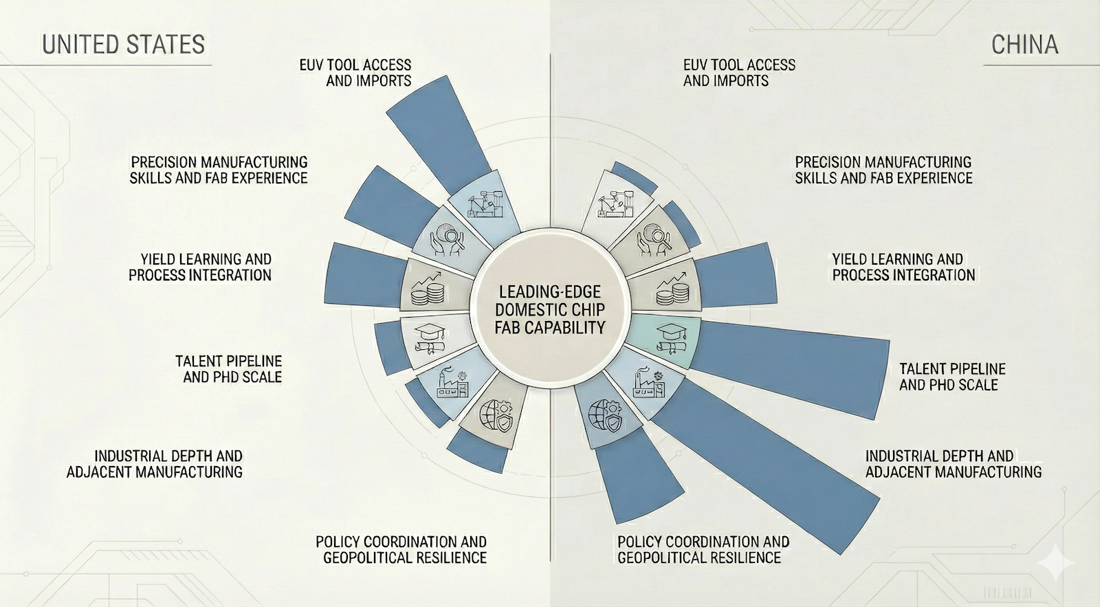 Google Gemini generated this comparative map of US and Chinese domestic semiconductor manufacturing capabilities, visualizing the stark asymmetry where American strength in advanced tooling contrasts with China’s advantages in industrial depth and long-term policy coordination.
China originally expected to gain access to EUV systems through the same commercial channels that had supplied earlier generations of chipmaking equipment. That assumption collapsed when the United States, under the Biden administration, assembled a coalition with key allies, including the Netherlands, South Korea and Japan, to block China from obtaining the most advanced chips and the tools required to make them. The intent was explicit: to slow China’s progress at the leading edge of semiconductor technology by denying access to EUV machines and related manufacturing capabilities. Once that path was closed, China faced a stark choice. It could accept permanent exclusion from the most advanced nodes of logic manufacturing, or it could attempt to recreate one of the most complex industrial systems ever built. The decision to pursue its own EUV capability was not based on confidence in rapid success, but on the recognition that without EUV, the most advanced chips would remain structurally out of reach.
The structure of the Chinese effort matters. This was not a single lab or company trying to replicate a Western product. It was a coordinated, multi-institution program that recombined capabilities already present across China’s research institutes, industrial suppliers, and manufacturing firms, with a top secret facility at the center of it. High-powered laser work was paired with plasma physics teams. Optical research groups worked alongside vacuum engineers and contamination specialists. Control systems expertise drawn from industrial automation and aerospace was adapted to nanometer-scale stability requirements. None of this was fast, and none of it was simple.
The foundation under this effort was human capital, and this was key to China’s ability to reverse engineer ASML EUV machines. Over the past two decades, China has produced a very large share of the world’s PhDs in the parent disciplines that feed EUV lithography and advanced chip manufacturing. Optics, photonics, materials science, plasma physics, control systems, and mechatronics are not niche fields in China. They are industrial-scale academic pipelines. Many of these PhDs were trained domestically in increasingly competitive programs. Many others were trained abroad in the United States, Europe, and Japan, then returned or remained connected through professional networks. The result is not a single cohort of experts, but overlapping generations of engineers capable of attempting problems that have no clear solution path.
This context explains why ASML became an inadvertent talent reservoir training Chinese nationals. ASML had no alternative but to hire globally and hence hire Chinese nationals. EUV lithography requires skills that exist in small numbers everywhere. Chinese nationals trained in elite universities were part of that pool, just as engineers from Europe, the United States, Japan, and elsewhere were, but in large numbers. This was not a failure of corporate governance. It was a reflection of how scarce expertise circulates in a global labor market. When China later assembled teams to work on EUV, it did not need thousands of people who had built EUV machines before. It needed hundreds who understood how such systems behave when theory meets production.
A useful way to ground this discussion is to look at the scale of the talent pipeline feeding EUV-era skills. China and the United States each award tens of thousands of doctoral degrees in science and engineering fields every year, with China having overtaken the U.S. in total S&E PhDs awarded around 2019 and continuing to grow that lead; in 2020 China awarded about 43,000 S&E doctorates while the United States was right behind with roughly 42,000, and more recent data suggest China’s annual STEM PhD total has continued rising above 50,000 compared to the U.S.’s roughly mid-30,000 range.
Another important factor is the composition of STEM education pipelines in the United States itself. Chinese nationals have been the single largest group of foreign students in US graduate STEM programs for many years, particularly in engineering, applied physics, materials science, and control-related fields that feed directly into advanced semiconductor manufacturing. In many top US programs, Chinese students make up a large share, and in some subfields a majority, of PhD candidates. These students contribute substantially to US research output while they are enrolled, but a significant fraction return to China after graduation or maintain professional ties that extend beyond the United States. The result is a structural drag on US PhD statistics in precisely the fields most relevant to EUV and leading-edge fabs. The United States trains a great deal of global talent, but captures a smaller share of it long term, which weakens the domestic accumulation of experience in these critical specialties even as headline PhD production numbers appear strong.
Within those broad totals, Chinese nationals likely account for roughly 25–40% of recent global PhD output feeding mechatronics and control engineering, about 20–35% in EUV source–relevant engineering and applied physics, and around 15–30% in precision optics and photonics, the three key specialty areas required for advancing EUV equipment. When taken together, these numbers imply that many thousands of Chinese-national PhDs are entering the global pool each year in these critical domains.
By contrast, companies like ASML employ on the order of 40,000 to 45,000 people worldwide, with around 15,000 to 17,000 engineers concentrated mainly in Europe, followed by the United States and Asia and only a small fraction located in China in service and support roles rather than core EUV R&D. The sheer volume of Chinese doctoral output in the relevant disciplines means that ASML had little practical choice but to hire Chinese nationals trained both in China and abroad, because they represent such a large share of the global skill pool in these rare specialties, and even relatively small flows of experienced engineers from that company into China link into a much broader national reservoir of adjacent and newly trained talent.
The United States is approaching semiconductor manufacturing from a different starting point. The CHIPS Act triggered a wave of announced and partially executed fab construction. Intel, TSMC, Samsung, Micron, and others are building or expanding facilities across multiple states. This is real progress. For the first time in decades, advanced semiconductor manufacturing capacity is returning to US soil at scale. The United States also retains a decisive advantage today. It can purchase EUV machines from ASML and deploy them in domestic fabs. That advantage, however, is geopolitical rather than structural.
Access to ASML tools depends on political alignment and export control regimes that are becoming more fragile over time. The same geopolitical tensions that motivated the CHIPS Act also create uncertainty around long-term access to the most advanced equipment. Even if access remains intact, buying tools does not solve the deeper problem of operating them at high yield, high uptime, and competitive cost. Fabs fail or succeed based on skills accumulated over years of production, not on the arrival date of equipment crates.
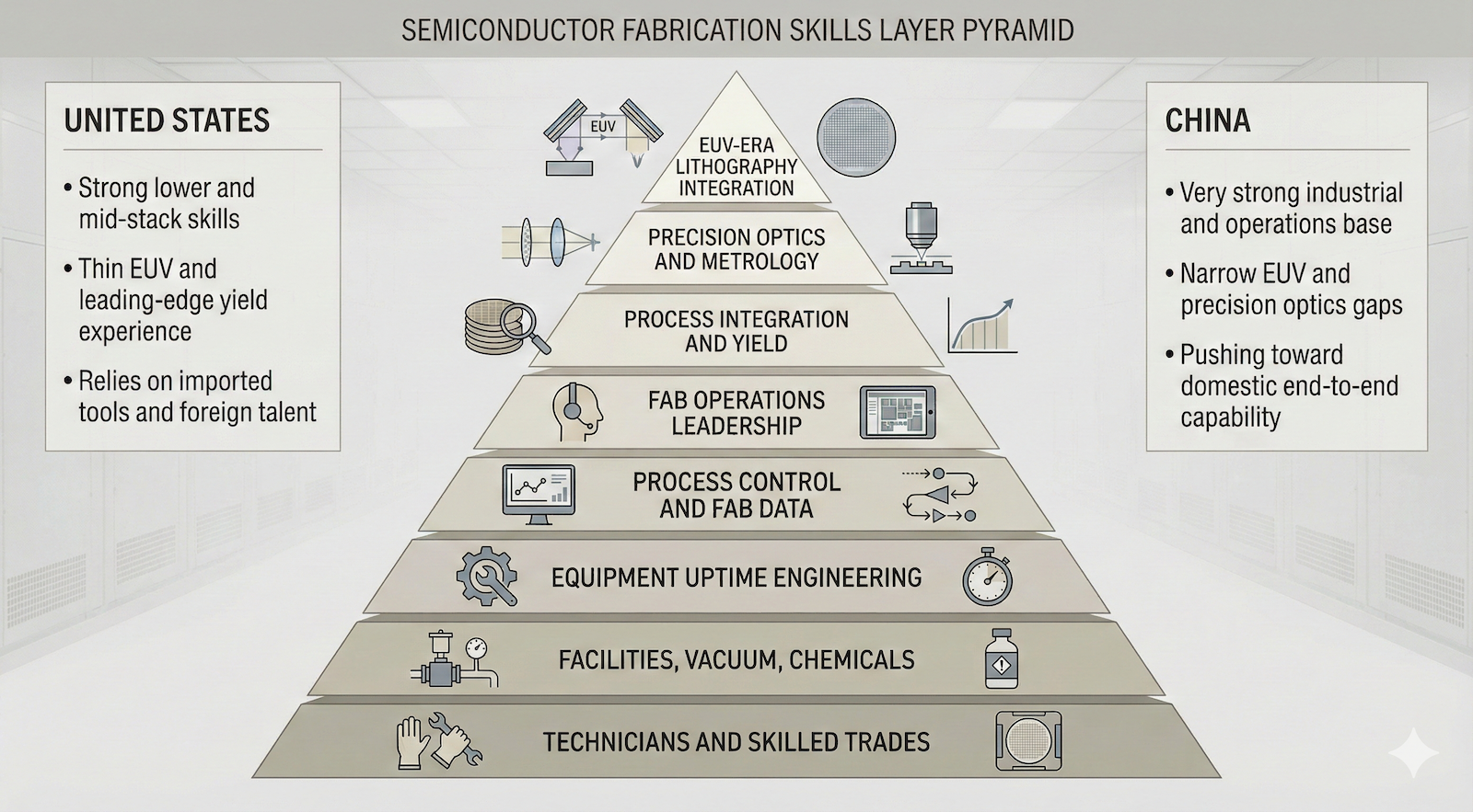 Visualization by TFIE Strategy, graphics by Google Gemini of the semiconductor fabrication skills pyramid, illustrating the operational hierarchy from foundational trades to advanced EUV integration while comparing the industrial readiness of the US and China.
This is where the skills stack matters. Semiconductor manufacturing capability can be understood as layered competencies. At the bottom are facilities, chemicals handling, vacuum systems, contamination control, technicians, and skilled trades. Above that sit equipment ownership, uptime engineering, process control, and manufacturing data systems. At the top are process integration, yield learning, precision optics, and advanced lithography integration. Each layer depends on the ones below it. Each layer also has a different learning curve.
To get a sense of what the competitive gaps are between the United States and China, I roughly rated across three dimensions, with a rating of one being worst and five being best. Current resource strength captures how much directly relevant experience exists today. Adjacent resource strength reflects how much transferable capability exists in nearby industries. Ease of bridging or foreign acquisition reflects how quickly gaps can be closed through retraining, hiring, or international talent flows. These ratings are not precise measurements. They are comparative judgments intended to clarify where time, not money, is the binding constraint.
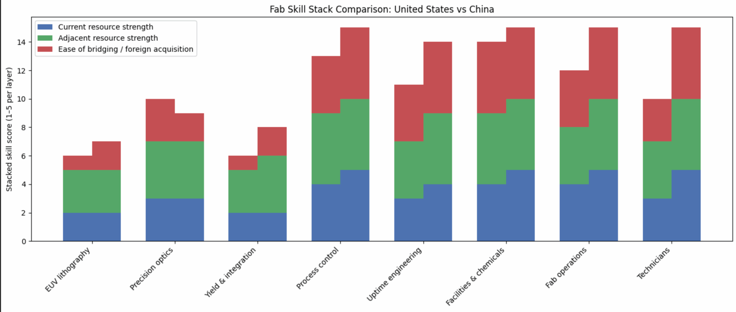 Chart contrasting skills gaps, adjacent skills and ability to bridge for China and United States by author
A comparative chart of the United States and China across these layers shows a consistent pattern. The United States scores well in facilities, controls, operations leadership, and adjacent industrial skills. It has deep experience in aerospace, chemicals, energy, automation, and high reliability systems. Where it scores poorly is at the top of the stack. Leading-edge process integration, yield learning at the most advanced nodes, and EUV-era lithography integration are thin because the United States has not run large numbers of leading-edge fabs continuously over the past decade.
China’s profile is different. Its current strength at the very top of the stack remains limited, but its adjacent strength is broader and its ability to staff, scale, and iterate is stronger across most layers. It runs many fabs at mature and mid-range nodes. It operates massive electronics manufacturing ecosystems. Its engineers are accustomed to high-volume production, rapid iteration, and long learning curves. The remaining gaps are narrow but difficult. Precision EUV optics, full system integration, and bleeding-edge yield learning are still constraints. They are also the same constraints export controls are designed to protect.
The difficulty of closing these gaps should not be underestimated for either country. You cannot train a yield engineer in six months. You cannot simulate years of uptime recovery experience. These skills emerge from repeated exposure to failure under production pressure. The United States faces this challenge while also making policy choices that reduce labor mobility. Attacks on skilled foreign workers, tighter visa regimes, and a more hostile environment for immigrants directly affect the ability to staff fabs with experienced personnel. That friction compounds over time.
China faces different risks. Its EUV effort shows persistence, but persistence does not guarantee success. Precision optics at EUV tolerances remain one of the hardest manufacturing challenges in the world. Integration failures can stall progress for years. Still, China’s trajectory matters more than its current position. It is systematically converting adjacent industrial strength into semiconductor capability, while the United States is attempting to rebuild capability that atrophied when manufacturing moved offshore.
The semiconductor race is not about who announces more fabs or who subsidizes more capital. It is about who can accumulate and retain the scar tissue required to run the world’s most complex manufacturing systems. The United States has advantages today, especially access to ASML and a strong base of adjacent skills. China, however, has a higher probability of building a fully domestic, high-performance chip manufacturing system over time because it is closing its hardest gaps while maintaining depth everywhere else. The outcome will be decided over decades, not election cycles, and it will be shaped more by people than by machines.
Sign up for CleanTechnica’s Weekly Substack for Zach and Scott’s in-depth analyses and high level summaries, sign up for our daily newsletter, and follow us on Google News!
Advertisement
Have a tip for CleanTechnica? Want to advertise? Want to suggest a guest for our CleanTech Talk podcast? Contact us here.
Sign up for our daily newsletter for 15 new cleantech stories a day. Or sign up for our weekly one on top stories of the week if daily is too frequent.
CleanTechnica uses affiliate links. See our policy here.