

Characterization of NbOI2 nanocrystals
Figure 1 a shows the crystal lattice of NbOI2. The lattice constants of NbOI2 are a = 15.18 Å, b = 3.92 Å, c = 7.52 Å, and the angle β between lattice vectors a and c is 105.50 ° 17. Bulk NbOI2 samples were grown using the chemical vapor transport (CVT) method (Methods). Figure 1b shows the Raman spectroscopy of bulk NbOI2, which revealed five distinct peaks at 105, 208, 273, 514, and 610 cm−1, in agreement with the previously reported values17. The thin samples used in UTED were mechanically exfoliated and transferred onto an amorphous Si3N4 thin film. As shown in Fig. 1c, the piezoresponse force microscopy (PFM) phase image confirms a uniform in-plane polarization in the exfoliated sample flake. Atomic force microscopy (AFM) was used to determine the sample morphology. Figure 1d shows the AFM topography image of an NbOI2 flake whose thickness ranges from 7.2 nm to 9.3 nm (Fig. 1e). The data presented in this work was primarily obtained from two samples with thicknesses of 39 nm and 7 nm, both with a lateral size of around 100 μm. The heat capacity of NbOI2 crystals was measured using a differential scanning calorimeter (DSC) to be 0.27 ± 0.04 J/(gK) at 20 °C and 0.31 ± 0.05 J/(gK) at 80 °C. The details of the PFM and DSC measurements can be found in supplementary materials (Sec. S-II).
Fig. 1: NbOI2 sample characterization and an overview of the experiment scheme.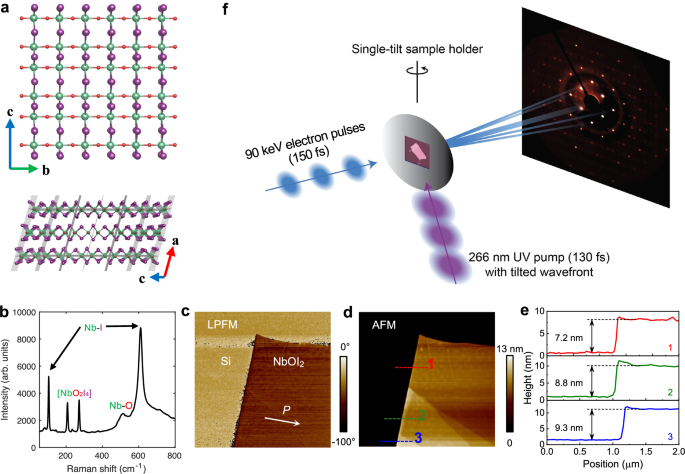
a A top view of one layer of the NbOI2 nanosheet (top) and a side view showing its monoclinic crystal lattice (bottom). b Raman spectrum of bulk NbOI2. The 105 cm−1 and 610 cm−1 peaks correspond to symmetric bending and asymmetric stretching of the Nb-I bond, respectively. Peaks at 208 cm−1 and 273 cm−1 arise from [NbO2I4] octahedron vibrations, while the 514 cm−1 peak reflects symmetric Nb-O bending. c LPFM phase image of the NbOI2 flake on Si with scanning angle of 10°, revealing a uniform in-plane polarization. d AFM topography image taken on an NbOI2 flake on Si wafer, with e the height profiles along the dashed lines. f An illustration of the experimental setup. The laser pump with 266 nm wavelength is incident on the sample at an angle of 58°. A 90 keV electron probe pulse of approximately 150 fs duration is scattered by the sample.
Transient deflection of pulsed electron beam
Figure 1 f illustrates the schematic of the UTED geometry. The samples, driven out of equilibrium using a 266 nm UV laser pulse with a fluence ranging from 0.5 to 1.4 mJ/cm2, are probed with 90 keV electron pulses of approximately 150 fs duration (full width at half maximum, FWHM) at a precisely controlled time delay. With a 200 Hz repetition rate, the samples are allowed enough time to relax to their original state after each repetition. Upon the laser excitation of the 39 nm sample, we observed a uniform shift of all diffraction orders in the same direction. Figure 2a shows the difference between the diffraction patterns taken at a 2 ps time delay and before the laser excitation, where the pixels with increased counts are displayed in red and those with decreased counts in blue. The differential image represents a uniform downward deflection of the entire diffraction pattern, and all Bragg peaks are deflected by the same angle on the detector. Such deflection occurs along the polar b-axis, which is marked by a green arrow in Fig. 2a. Figure 2b shows the time-resolved motion averaged over the eight brightest diffraction orders, where the relative positions-referenced to their pre-excitation locations-are converted into electron deflection angles as a function of pump-probe delay. A zoomed-in scan with finer time steps over a shorter range is shown in the inset. In less than 2 ps, the deflection of all Bragg orders reaches the maximum, followed by a recovery in the next 20 ps. The deflection changes direction and continues to increase until around 50 ps. Subsequently, a slower relaxation extends over hundreds of picoseconds.
Fig. 2: Ultrafast deflection dynamics of the electron beam.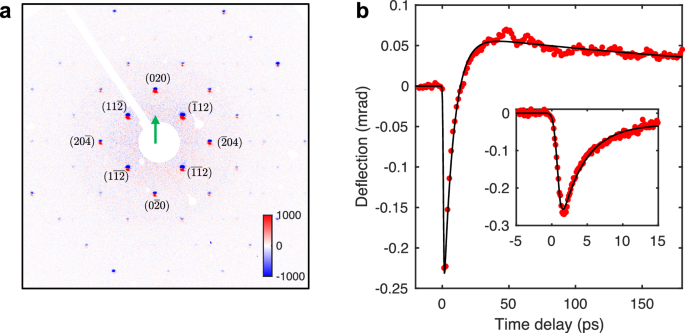
a A differential image between the electron diffraction patterns taken at 2 ps after laser excitation and before the arrival of laser pulses. The green arrows mark the polar b*-axis. b Averaged time-resolved deflection of the low-order \(\{11\overline{2}\}\), {020} and \(\{20\overline{4}\}\) Bragg peaks. The inset depicts a scan with finer temporal resolution over a 15 ps pump-probe delay range.
We attribute the time-dependent deflection of the Bragg peaks depicted in Fig. 2b to a change in the polarization of the sample. The movement is independent of the diffraction order, ruling out the possibility of it being driven by changes in the lattice parameters. Additionally, the movement is along the polar axis of the sample, along which a spontaneous electric field exists. The shifting of Bragg peaks results from the time-dependent deflection of the electron beam within the sample, induced by an evolving electric field inside the polarised crystal.
To verify that the electron beam is deflected by the ferroelectric polarization, we performed selected area electron diffraction (SAED) using a transmission electron microscope (TEM) (Fig. 3a) without laser excitations. The sample consists of a 10 nm-thick single-crystal NbOI2 flake, which is deposited on top of a single-crystal silicon substrate of 15 nm thickness. The transverse size of the sample is small compared to the substrate. Thus, we can compare the diffraction from the sample and substrate together with the diffraction from the substrate only. Electrons diffracted through the polarized crystal are expected to acquire an additional deflection compared to those traversing only the substrate. We designed a selected area consisting of both the deflected and undeflected electrons, which is shown in Fig. 3b, where half of the electron beam interacts with both the NbOI2 sample and the silicon substrate, while the other half interacts only with the silicon substrate. The resulting SAED pattern displayed in Fig. 3a suggests that the Bragg peaks of the silicon thin film (circled in red) are split along the polar axis by 0.24 mrad in this diffraction geometry. In contrast, as shown in Fig. 3c, selecting a region containing only the silicon substrate results in unsplit Bragg peaks. The disparity in the splitting of silicon Bragg peaks, with and without the NbOI2 sample, clearly demonstrates the polarized crystal deflects a keV electron beam by a measurable angle. A quantitative analysis (Sec. S-I) of the deflection angle gives an intrinsic electric field of 8 × 10⁹ V/m, matching the intrinsic field of 9 × 10⁹ V/m, calculated from the polarization and dielectric constants of NbOI219.
Fig. 3: Static deflection of electron beam investigated with transmission electron microscopy.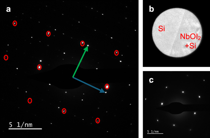
a An SAED pattern consisting of Bragg peaks from both the NbOI2 sample and the single-crystal silicon substrate. The green and blue arrows mark the polar and non-polar axes, respectively. The diffraction from silicon is circled in red and split along the polar axis. b The selected area where diffraction pattern in (a) is taken. c A reference SAED pattern taken from the silicon substrate only.
Domain dynamics are confirmed to have no influence on the experimental results based on three reasons. First, the PFM measurements performed on several freshly exfoliated NbOI2 samples with lateral size on the order of 100 μm show a uniform polarization with no domain walls (Sec. S-II). Second, in the UTED experiments, the pump fluence is capped so that the thermalized temperature of the samples is below the Curie temperature of 189 °C19. Third, the effect of domain structures in NbOI2 samples would be to split or elongate the Bragg peaks along the polar axis due to the opposite directions of electric fields. Such an effect was not observed.
Ultrafast suppression of ferroelectric order
The changes in polarization, as seen in Fig. 2b, have three distinct time scales: 1. From excitation up to 2 ps, the diffraction orders move and reach a maximum deflection angle. 2. Over the next 50 ps, the deflection angle recovers towards zero and overshoots in the opposite direction. 3. Subsequently, a slower relaxation on the timescale of more than a hundred picoseconds occurs. The deflection angle of the electron pulse is phenomenologically described as:
$$\Delta S={A}_{1}\,{{{\rm{erfc}}}}\,\left(\frac{t-{t}_{1}}{{\tau }_{1}}\right)+{A}_{2}\,\exp \left(-\frac{t-{t}_{2}}{{\tau }_{2}}\right)\cdot \exp \left(-\frac{t-{t}_{3}}{{\tau }_{3}}\right)+C,$$
(1)
where a complementary error function with time constant τ1 represents the rapid suppression of polarization; two exponential terms with time constants τ2 and τ3 describe the recovery and the slow relaxation. A fit of equation (1) to the data (Fig. 2b) returns the time constants τ1 = 0.679 ps, τ2 = 7.75 ps and τ3 = 299 ps. At the maximum delay time of 178 ps, the deflection angle remains above zero. Considering the relatively long recovery time, it is safe to assume the enhanced polarization will persist for several hundred picoseconds.
In the first two picoseconds, the polarization of the samples is rapidly suppressed by two factors: a rapid lattice temperature rise and carrier charge screening. As shown in Fig. 4a, the ultrafast lattice heating is evidenced by the intensity reduction of the (020) diffraction order, observed in the 39 nm and 7 nm thick samples, corresponding to inhomogeneous and homogeneous heating, respectively. Based on a reported imaginary dielectric coefficient ε2 of 6.4 for 266 nm UV laser25, we estimate the absorption length of the pump pulse to be 10 nm. In the 7 nm-thick sample, the dynamics resemble the Debye-Waller effect, and the temperature rise is mostly uniform across its thickness. The diffraction intensity continuously decreases until the lattice temperature reaches a maximum at around 7 ps. In the thick sample, the Bragg intensity also sees a rapid suppression in the first 2 ps, after which the dynamics are dominated by the strain wave. In both cases, the temperature of the lattice rapidly increases in the first 2 ps, which matches the timescale for the initial change in the polarization depicted in Fig. 2b.
Fig. 4: Ultrafast structural dynamics depicted by the Bragg diffraction intensity and peak width.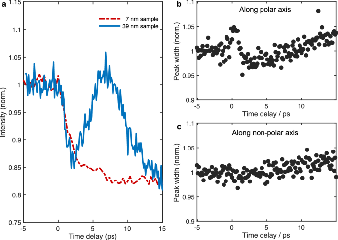
a The normalized Bragg peak intensity of the (020) diffraction order from a 7-nm sample (red dashed line) and a 39-nm sample (blue line). b The normalized peak width along the polarized axis taken from the 39-nm sample. c The normalized peak width along the non-polar axis taken from the 39-nm sample. A broadening of the Bragg peak occurs in the first picosecond along the polar axis, which is absent along the non-polar axis.
Another contributing factor to the reduction of polarization is the charge screening effect. The absorption of the femtosecond pump pulse generates hot carriers, and the creation and relaxation dynamics of hot carriers in NbOI2 are evidenced by the time-resolved reflectivity measurements performed by Huang et al.23. The increased carrier population leads to the screening of the internal polarization field1,6 and the emission of coherent acoustic phonons. Figure 4b, c show the normalized FWHM of the (020) diffraction order in the 39 nm sample along the polar and non-polar axes, respectively. A broadening of the Bragg peak along the polar axis is found in the first picosecond after laser excitation, which is absent along the non-polar axis. The anisotropic broadening of the Bragg peak suggests it is unrelated to lattice heating. The broadening of the Bragg peak along the polar axis results from an uneven screening of the internal polarization field along the thickness dimension of the sample. In the 39 nm sample, a gradient of electron temperature is created after the absorption of the laser pump pulse, leading to a depth-dependent dampening of the intrinsic electric field in the sample. As a result, a minor smearing of the electron beam is caused along the polar axis. At maximum, the smearing reaches 0.01 mrad in real space, which is much smaller than the deflection (0.27 mrad at maximum) and occurs only within the first picosecond, indicating it cannot result from domain dynamics.
In the following picosecond, the smearing of the internal polarization field vanishes, which is likely a result of the thermalization of the carrier system via electron-electron scattering across layers of the 2D sample. Coherent strain waves form and dominate the dynamics after 2 ps, exerting a significant influence on the sample’s polarization due to its strong piezoelectric response.
Laser-induced strain dynamics
Coherent acoustic waves are launched along the thickness of the sample due to the transiently increased thermal stress in the electronic and lattice systems, charge screening, and inverse piezoelectric response36,37,38,39,40,41,42. As depicted in Fig. 2b and Fig. 4, the effects of acoustic waves on the diffraction pattern are clearly observable after 2 ps. The polarization changes from a rapid reduction to a fast recovery; the thermal suppression of Bragg diffraction intensity is overtaken by the modulation from lattice deformation in the presence of the acoustic wave; the Bragg peak width gradually increases after 2 ps, as part of a longer oscillatory behavior induced by the acoustic wave, which has a substantially longer period.
The interlayer lattice motions induced by the acoustic waves are examined by the time-resolved intensity and FWHM of the Bragg peaks from the 39 nm-thick sample, shown in Fig. 5a, b. The diffraction intensities of a Friedel pair consisting of (\(\overline{1}12\)) and (\(1\overline{12}\)) diffraction orders oscillate at 20 GHz with opposite phases (Fig. 5a). The anti-symmetric phase distribution about the polar axis is displayed in Fig. 5c. This phenomenon is attributed to the time-varying, antisymmetric excitation error in the diffraction geometry, caused by the rotation of the reciprocal lattice. Figure. 5d illustrates such wobbling motions of the reciprocal lattice. In momentum space, a seesaw motion occurs in the reciprocal lattice due to the shear acoustic wave, causing the diffraction orders on the left to deviate from the Bragg condition while those on the right shift towards it. The seesaw motion of the reciprocal lattice can be further demonstrated by the evolution of the Bragg peak width, which oscillates on the same 20 GHz frequency. Figure 5b shows the FWHM of the \((4\overline{28})\) diffraction order, where the larger wavevector causes a significant deviation from its Bragg condition, resulting in weaker diffraction intensity under static conditions. Under the influence of the shear wave, the diffraction geometry for the \((4\overline{28})\) diffraction order periodically gets closer to and away from the Bragg condition, with its FWHM changing accordingly.
Fig. 5: Anti-symmetric oscillations induced by coherent acoustic waves.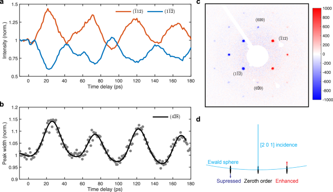
a The diffraction intensity of the (\(\overline{1}12\)) and (\(1\overline{12}\)) orders. b The temporal evolution of the FWHM of \((4\overline{28})\) diffraction order along the polar axis. c A differential image showing the diffraction pattern taken at 25 ps delay time, subtracting the diffraction pattern taken before the arrival of the laser pulse. d, The Ewald sphere of the 90 keV electrons. A seesaw motion in the reciprocal lattice causes the antisymmetric modulation to the Bragg condition of a Friedel pair.
In the thicker sample, where the laser’s absorption length is significantly smaller than the crystal’s thickness, the acoustic waves are launched as traveling blast waves along the sample’s thickness dimension. The wavefront of the acoustic wave is reflected at the bottom of the sample, and the reflected wave propagates upward. The oscillation frequency is determined by the sound velocity and the thickness of the sample: f = v/2D, where v is the interlayer sound velocity and D is the sample thickness. Further discussions of the modes of acoustic waves may be found in the supplementary materials (Sec. S-IV). The traveling acoustic wave cools the hotter lattice layers by transferring heat across the longitudinal dimension of the sample, which leads to a fast recovery of the average polarization. As depicted in Fig. 2b, the thermal relaxation of the thermalized NbOI2 lattice happens subsequently. It spans out into hundreds of picoseconds, which fall into the timescale of thermal relaxation via diffusion into the substrate. During this time, the oscillations in the intensity and width of Bragg peaks continue with a decreasing amplitude.