
Flexible dual-mode synaptic device based on a bilayer dielectric structure
Figure 1a shows the structure of the proposed dual-mode device fabricated on a flexible business card substrate, which provides both memory and synaptic functions within a single device. The device with a bottom-gate, top-contact (BGTC) geometry features bilayer dielectric structure where pBDDA and Parylene were employed as a blocking dielectric layer (BDL) and tunneling dielectric layer (TDL), respectively, and dinaphtho[2,3-b:2′,3′-f]thieno[3,2-b]thiophene (DNTT) was utilized as a channel layer. Both dielectric layers were fabricated by using CVD processes to enable the consecutive deposition of high-purity polymer dielectric films. Among them, the pBDDA layer was deposited via an initiated chemical vapor deposition (iCVD), an all-dry process that enables the formation of high-purity polymer thin films without the use of solvents or additives46. The iCVD process involves in-situ free-radical polymerization occurring at the substrate surface, which allows for the conformal and uniform deposition of highly crosslinked polymeric films even at ultrathin thicknesses40. Given its low processing temperature with the substrate maintained near room temperature throughout the process, this technique is suitable for thermally vulnerable flexible substrates, such as business cards. The resulting pBDDA film, with its highly crosslinked polymer network, exhibited excellent insulating properties, including extremely low leakage current and high breakdown field42. These characteristics effectively suppress gate leakage and prevent dielectric breakdown under programming conditions. For these reasons, pBDDA serves as an ideal BDL material in memory transistors, ensuring reliable operation and improved stability under repeated high-voltage stress. Meanwhile, Parylene was employed as the TDL, as it has been widely used in electronic devices due to its excellent electrical properties47,48. In particular, its compatibility with the CVD process allows for effective suppression of both bulk and interface trap densities, and facilitates the formation of a well-defined bilayer structure by preventing intermixing between dielectric layers. The cross-sectional scanning electron microscope (SEM) image confirmed that pBDDA and Parylene were deposited in a layer-by-layer structure with thicknesses of 300 and 50 nm, respectively (Fig. 1b). Fourier transform infrared (FT-IR) spectra of pBDDA and 1,4-butanediol diacrylate (BDDA) are shown in Supplementary Fig. 1. The peak at the wavenumber ranging from 1650 to 1606 cm−1 corresponding to the C\(=\)C stretch of the vinyl bond, disappeared in the FT-IR spectrum of pBDDA in comparison to that of BDDA. Meanwhile, the peaks at 1719 and 1179 cm−1, which correspond to the C=O and C−O−C bonds, respectively, were fully preserved in the FT-IR spectrum of pBDDA. The FT-IR analysis suggested that free-radical polymerization was successfully achieved by the iCVD process while maintaining functional groups in the monomer species.
Fig. 1: Structure and operation principles of the dual-mode organic neuromorphic device.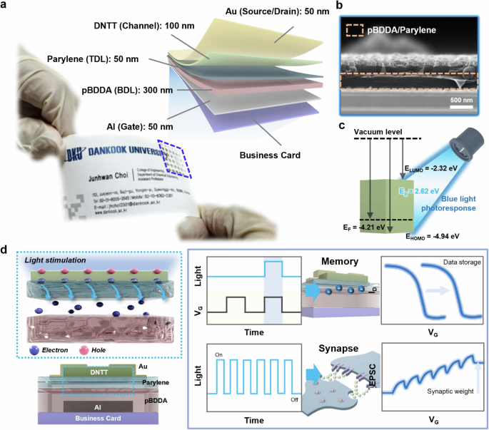
a Schematic illustration of the dual-mode device fabricated on a business card. b Cross-sectional SEM image of the device. c Energy band diagram of DNTT, indicating the Fermi level, HOMO, LUMO, and optical band gap. d Schematic representation of the input-dependent memory and synaptic operations induced by charge trapping at the interface between pBDDA and Parylene of the dual-mode device.
To investigate the optical properties and energy band structure of DNTT, which plays an important role in generating the carriers for both memory and synaptic functions, ultraviolet-visible (UV-vis) spectroscopy analysis was performed. As shown in Supplementary Fig. 2a, DNTT exhibited strong absorption at the wavelength of 471 nm and the corresponding optical band gap was determined to be 2.62 eV from the Tauc plot (Supplementary Fig. 2b). Additionally, the secondary cut-off and valence band edges of DNTT were measured to be 16.99 and 0.73 eV, respectively, in the ultraviolet photoelectron spectroscopy (UPS) analysis (Supplementary Fig. 2c). According to the UV-vis and UPS analyses, the energy band diagram of DNTT was determined, with a Fermi level of −4.21 eV, a lowest unoccupied molecular orbital (LUMO) of −2.32 eV, and a highest occupied molecular orbital (HOMO) of −4.94 eV (Fig. 1c). Based on the energy band structure of DNTT, we utilized blue light to induce the photoresponse of DNTT, thereby facilitating the photoinduced charge trapping effect. The bilayer dielectric stack in the dual-mode device also enabled this charge trapping behavior in which the photogenerated electrons in DNTT are stored at the interface between pBDDA and Parylene through tunneling, successfully realizing two different types of optoelectronic applications: memory and synaptic characteristics (Fig. 1d). The combined optical and electrical signals allowed for the charge storage by instantaneously accumulating significant amounts of charge carriers, leading to the memory characteristics. On the other hand, synaptic behavior was demonstrated with gradual charge accumulation by optical pulses.
Memory operation of a dual-mode device via simultaneous optical and electrical inputs
The memory operation of the dual-mode device was achieved through the accumulation of photogenerated carriers at the interface of the bilayer dielectric, with the assistance of an electrical signal, as shown in Fig. 2a. For programming operation, both VG and light with wavelength of 455 nm were applied simultaneously to the device. The transfer curve was shifted toward positive VG direction by applying VG of 50 V and a light intensity of 0.19 mW∙cm−2 for 2 s (Fig. 2b). The programmed state (P-state) was enabled by charge trapping of photogenerated electrons, and this interpretation was supported by the observation that only a marginal shift in the transfer curves occurred when either electrical or optical input was applied separately (Supplementary Fig. 3). Meanwhile, only a VG was used for erasing operation, without the need of photoinduced carrier generations. The erased state (E-state) was attained by applying a VG of −50 V for 2 s to the programmed dual-mode device, which is practically identical to the initial state (I-state) (Fig. 2b). For a quantitative analysis of the memory characteristics, the memory window was calculated using the following equation:
$$M{emory\; window}\left(V\right)={V}_{p}-{V}_{i}$$
(1)
where \({V}_{p}\) and \({V}_{i}\) refer to the VG values corresponding to the pre-defined drain current value (ID = 1 nA) in the P-state and I-state, respectively. The memory window obtained by the combined VG and light input signals was 11 V (Fig. 2c). On the contrary, when using only voltage input or only light input, the memory window was limited to 1 V and 2 V, respectively. In other words, both electrical and optical signals are required to achieve sufficient memory window, which is fully consistent with our interpretation on charge trapping behavior of the photogenerated electrons. Moreover, the charge storage capability was demonstrated due to the distinctive properties of pBDDA/Parylene bilayer dielectric structure, eliminating the need for an additional charge trapping layer, which is beneficial for simplifying the device structure.
Fig. 2: Dual-mode memory operations enabled by electrical and optical inputs.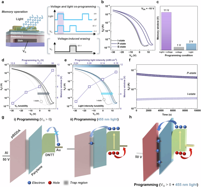
a Schematic representation of memory operation of the dual-mode device using both light and electrical input signals. b The change in transfer curves depending on programming and erasing operation where the VD was fixed at −10 V. c The change in memory window according to programming conditions. The programming operation was performed by applying light intensity of 0.19 mW∙cm−2 and/or VG of 50 V to the device. d VG-dependent and e light intensity-dependent programming operation and memory window of the device. f The change in ID in P- and I-states with respect to time at VG of 0 V. The VG and VD values were fixed at 0 and −10 V, respectively. g Energy band diagrams for programming operations by separately applying VG (left) and light (right). h Energy band diagram for programming operation by using both VG and light.
The tunability of the memory window was further investigated by adjusting the applied VG and light intensity. When VG applied to the device varied from 12.5 to 50 V in 12.5 V step at the fixed light intensity of 0.19 mW∙cm−2, the transfer curves were gradually shifted with the increasing VG (Fig. 2d). The memory windows were measured to 5, 7, 8, and 11 V according to the applied VG values of 12.5, 25, 37.5, and 50 V, respectively, in the programming operation. Similarly, the memory window continuously increased from 7 to 11 V with the increasing light intensity from 0.04 to 0.19 mW∙cm−2, at the fixed VG of 50 V (Fig. 2e). In the erasing operation, the transfer curve shifted in the opposite direction from the P-state, and this shift also occurred gradually depending on the magnitude of the applied negative VG (Supplementary Fig. 4). Additionally, we analyzed the retention characteristics of the device (Fig. 2f). The measured ID values at the VG of 0 V and drain voltage (VD) of −10 V in the P- and I-states were preserved for 10,000 s. Specifically, the ID in the P-state changed from 63.9 to 48.5 nA after 5000 s and was ultimately maintained at 41.5 nA after 10,000 s, demonstrating robust charge storage capability through the interface between the polymeric layers.
To provide deeper understanding for the memory operation in the proposed dual-mode device, we investigated charge injection, transport and trapping in the energy band structure (Fig. 2g and Supplementary Fig. 5). In this configuration, the two dielectric layers play distinct roles in facilitating interfacial charge trapping. The Parylene TDL allows photogenerated electrons in the DNTT channel to tunnel through, under the combined influence of optical and electrical input. Meanwhile, the pBDDA BDL effectively suppresses gate leakage and preserves the stored charges by preventing carrier transport toward the gate electrode. This interfacial trapping mechanism enables a stable charge storage without the need for a floating gate, thereby realizing both memory and synaptic functionalities in the dual-mode device. Hole carriers are predominantly present in p-type DNTT semiconductor, whereas high energy barrier between Au source/drain (S/D) electrodes and DNTT is present for electron carriers. Thus, with the absence of the injected electrons, electron trapping at the interface between pBDDA and Parylene hardly occurs even when a sufficiently high positive VG (50 V) is applied (Fig. 2g (left)). Accordingly, bias-induced programming is significantly restricted, which is consistent with the negligible shift in transfer curves in voltage-induced programming operation (Supplementary Fig. 3a). On the other hand, light irradiation with a wavelength of 455 nm can effectively generate electron-hole pairs in DNTT. Nevertheless, with the absence of the applied bias, energy band bending is insufficient to induce charge trapping at the pBDDA/Parylene interface (Fig. 2g (right)), leading to the subtle shift in transfer curve (Supplementary Fig. 3b). When the light and positive VG were applied, which induced electron carrier generation in DNTT and appropriate band bending, respectively, trapping of the photogenerated electrons is enabled (Fig. 2h). In other words, based on trap sites at the pBDDA/Parylene interface and photoresponse of DNTT, memory programming operation in the dual-mode device can be implemented by utilizing both light irradiation and voltage application. Thus, the memory window could be systematically tuned depending on the applied voltage and light intensity, while maintaining robust retention characteristics.
Synaptic operation of a dual-mode device triggered by optical stimulation
In addition to the memory behaviors, synaptic characteristics were also implemented in the proposed dual-mode device, by using the photoinduced charge trapping effect in the bilayer dielectric structure. To activate the synaptic behavior for emulating biological synapses, both optical and electrical stimulation were applied as presynaptic inputs, and the postsynaptic output was extracted based on the ID value (Fig. 3a). In particular, consecutively applied optical pulses gradually amplify electron trapping at the pBDDA/Parylene interface, which can be regarded as synaptic potentiation. In this process, the photogenerated electrons tunnel through the Parylene layer, while the holes migrate to the drain electrode of the device. As a result, excitatory postsynaptic current (EPSC) increases due to the enhanced photogating effect as optical stimulation continues. Conversely, synaptic depression occurs as electrons are progressively detrapped from the pBDDA/Parylene interface into the DNTT channel through VG pulses.
Fig. 3: Synaptic functionalities of the dual-mode device enabled by optical and electrical stimuli.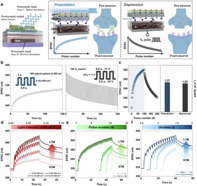
a Schematic representation of the synaptic operation of the dual-mode device including potentiation and depression via optical and VG pulses, respectively, based on charge trapping effect at the pBDDA/Parylene interface. b Potentiation–depression curve obtained by using optical (left) and electrical stimulation (right). c The change in EPSC according to the number of pulses and quantitative assessment of synaptic weight change. Synaptic weight modulation as a function of d light intensity, e pulse number, and f on-time through optical stimulation.
In the memory operation, both optical and electrical inputs were required to facilitate substantial charge trapping (Fig. 2g). In contrast, data transmission and processing are promoted by the gradual modulation of neurotransmitter movement in response to external stimuli in the synaptic behavior in nervous system. Consequently, light-generated synaptic weight by activating the device, while voltage weakened the synaptic connection, successfully emulating this behavior.
Figure 3b shows the potentiation–depression curve obtained in the synaptic operation of the dual-mode device, describing synaptic plasticity. Synaptic potentiation, represented by an increase in EPSC was achieved by using a total of 100 optical pulses with on-time for 1 s, off-time for 0.5 s, and an intensity of 0.18 mW∙cm−2, whereas VG pulses alternating between −10 V and −11 V every 0.5 s induced a decrease in EPSC, corresponding to synaptic depression. To qauntitatively evaluate the synaptic connection in terms of the potentiation–depression characteristics, synaptic weight changes were evaluated by extracting EPSC for each presynaptic input pulse and by using the following equation:
$$S{ynaptic\; weig}ht\,ch{ange\; for\; potentiation}\left(A\cdot {A}^{-1}\right)={W}_{100}/{W}_{1}$$
(2)
$$S{ynaptic\; weig}ht\,ch{ange\; for\; depression}\left(A\cdot {A}^{-1}\right)={W}_{1}/{W}_{100}$$
(3)
where Wn denotes the EPSC value at the nth pulse. Using the equation, synaptic weight changes were found to be 1.37 A ∙ A−1 and 1.22 A ∙ A−1 for potentiation and depression, respectively (Fig. 3c). These comparable values suggested that strengthening EPSC through optical stimulation can be counteracted by electrical stimulation, nearly restoring the synaptic weight to its initial state.
Two different mechanisms contribute to data processing in the nervous system, serving different functions. Short-term memory (STM) enables rapid responses to new stimuli and facilitates information filtering, whereas long-term memory (LTM), established via sustained and repetitive stimuli, enables long-term data storage and influences future behaviors and decision-making through learning. The proposed dual-mode device successfully mimicked these synaptic operations by modulating charge trapping in response to varying optical stimulation conditions. As shown in Fig. 3d–f, the transition from STM to LTM was achieved by adjusting optical stimulation parameters, including light intensity, number of pulses, and duration for light irradiation. Stronger light intensity induced a greater increase in EPSC compared to weaker one, and this trend persisted even after the optical stimulation was removed. Similarly, EPSC values increased proportionally with respect to the increasing number of pulses and on-time. Consequently, synaptic connection was enhanced or weakened depending on the conditions of the optical stimulation and our proposed device demonstrates the ability to mimic both transient and persistent synaptic behavior by light stimulation, which verifies its versatile potential for neuromorphic hardware applications49.
Fingerprint recognition-based identification classification and evaluation for flexible optoelectronic application
We applied our device to fingerprint recognition for identification (ID) classification, utilizing its ability to emulate synaptic characteristics and process data patterns. Fingerprint recognition is a widely used biometric modality for human identification, owing to its unique and consistent pattern. Based on these advantages, it is extensively applied in fields such as financial payment systems, secure authentication of electronic devices, and access control, among others. In recent years, artificial neural network (ANN)-based fingerprint recognition system has garnered significant research interest because of its robustness against noise and deformation, high accuracy, and system adaptability50,51. Conventional fingerprint recognition methods depend on explicitly defined feature point extraction and matching algorithms, which are susceptible to environmental variations such as changes in orientation, incomplete ridge impressions, and low-quality images52,53,54. In contrast, our ANN based on the dual-mode device enables adaptive learning and robust fingerprint recognition under challenging conditions such as rotation, partial fingerprints, and degraded image quality. To conduct the fingerprint recognition simulation, we used the long-term potentiation/depression (LTP/D) characteristics of the dual-mode device and designed the ANN consisting of an input layer with 4096 neurons, a hidden layer with 128 neurons, and an output layer with 10 neurons (Fig. 4a). For ID classification, fingerprint data from 10 individuals were used, with individuals representing distinct classes (i.e. 10 classes), and labels ranging from 0 to 9 were assigned to each class (Supplementary Fig. 6a). The ANN was then examined using the fingerprint dataset for 10 classes consisting of 50,000 training and 10,000 testing images. Figure 4b shows the simulation result over 30 training epochs. The average accuracy exceeded 90% and the maximum accuracy was 96% for 30 epochs. In the confusion matrix, the true ID (i.e. label) closely matched the predicted ID, which was obtained through the synaptic operation-based ANN training (Supplementary Fig. 6b). These results demonstrate the strong potential of the proposed dual-mode device to develop an authentication and security platform for matching a personal fingerprint with stored data. Moreover, such fingerprint recognition can further enhance the functionality of business cards, and the strong compatibility with paper substrates highlights the broad applicability of the proposed device across various fields.
Fig. 4: Fingerprint recognition application and mechanical reliability of the dual-mode device.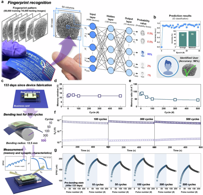
a Schematic representation of fingerprint recognition-based ID classification using the proposed device. b Accuracy according to epoch for fingerprint recognition simulation. c Schematic representation of the comprehensive bending test for 500 cycles. d The change in memory window and e memory ratio over bending cycle. f The change in ID according to time after applying 100, 300, and 500 bending cycles. g The change in potentiation–depression curves as a function of bending cycle.
To further evaluate the performance of the dual-mode device, we conducted a comparative analysis of recently reported organic synaptic transistors, including the proposed device55,56,57,58,59. Supplementary Table 1 summarizes key comparison metrics such as device structure, weight-update signals, dynamic range, number of conductance states, recognition accuracy, and the ANN model. In particular, synaptic weight changes are represented by the dynamic range in Supplementary Table 1. While most previous studies report the dynamic range as a combined value across the full potentiation–depression curve, in this study, we separately extracted and reported the values for potentiation and depression. As a result, the dynamic range of the dual-mode device was lower than those reported in previous studies. However, the fingerprint recognition simulation still achieved a high accuracy of 90%, demonstrating competitive performance relative to prior reports (approximately 75%–93%). Furthermore, the dual-mode device successfully performed image recognition on a business card, highlighting its potential for applications in flexible optoelectronics.
Organic materials, known for their high suitability for flexibility and stretchability, offer a wide range of potential applications, including skin electronics and wearable devices60. The dual-mode device was fabricated using organic components (DNTT, Parylene, and pBDDA) to ensure stable operation when integrated onto a business card. Thus, we investigated its performance under the applied mechanical strain to evaluate the viability for flexible optoelectronics (Supplementary Fig. 7). Figure 4c outlines the comprehensive process of the bending test, which evaluates both the mechanical durability and ambient stability of the device. Initially, the memory and synaptic characteristics of the dual-mode device were examined in the pre-bending state, 133 days after device fabrication. The device was then subjected to 500 bending cycles using a cylindrical bar with a bending radius of 12.5 mm. We measured the memory and synaptic characteristics after 10, 50, 100, 300, and 500 cycles to assess the consistency of the device performance throughout the bending experiment. The memory operation showed stable behavior, and memory windows and memory ratios measured at VG of 0 V remained reliable after 500 bending cycles (Fig. 4d, e). Memory ratio was calculated by the following equation:
$$M{emory\; ratio}\left(A{\cdot A}^{-1}\right)={I}_{p}-{I}_{i}$$
(4)
where \({I}_{p}\) and \({I}_{i}\) refer to the ID values corresponding to the pre-defined VG value of 0 V in the P-state and I-state, respectively. In the retention characteristics, the clearly distinguishable P- and I-states were preserved even after 500 bending cycles over 600 s, indicating that the device composed of the organic materials (pBDDA, Parylene, and DNTT) are well-suited for flexible optoelectronics (Fig. 4f). Additionally, the synaptic characteristics under cyclic mechanical deformation were analyzed, where reliable potentiation–depression curves were obtained, as shown in Fig. 4g. To further support the mechanical deformability of our device, fingerprint recognition simulation was performed in the same manner. Supplementary Fig. 8 shows that similar accuracies were maintained under the bending cycles with reliable recognition of fingerprint images where the average accuracies in pre-bending state and after 500 cycles were 89% and 85%, respectively. This slight degradation in accuracy can be attributed to variations in the potentiation–depression curves under identical stimulation, resulting from changes in charge trapping and detrapping dynamics induced by repeated mechanical strain. The confusion matrices also exhibited reliable potential for ID recognition on a business card, confirming consistent ability of the device to classify fingerprint images under mechanical stress (Supplementary Fig. 9).