
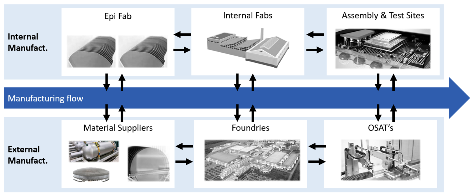
An explosion in data from inspection images and metrology measurements is creating a confusing set of demands for chipmakers and their equipment vendors. On one hand they need the massive storage and compute resources of the cloud to utilize AI/ML-based models, but they also need the faster response time of the edge to make adjustments at the tool level.
Balancing these requirements is a massive and costly challenge. It requires access to both upstream and downstream data, as well as refined machine learning models. The goal is to ship only high-quality data to the cloud, where huge amounts of data can be efficiently processed using ML algorithms. That, in turn, allows decision models to deliver the precision and accuracy needed for high-speed inspection and for metrology purposes. At the same time, this also requires increased investments in data storage and compute resources at the inspection/metrology tool level, the factory level, and at the cross-facility level.
Machine learning has been creeping into inspection and metrology for the past few years, but the integration of cloud and edge data is a new development. ML has proven to be effective across a range of semiconductor processes, including optical, e-beam, X-ray, infrared, and acoustic inspection, for the measurement and inspection of reticles, wafers, IC substrates, packages, and PCBs.
“Our inspection systems capture and identify defects on wafers, reticles, packages, IC substrates, and PCBs,” said a KLA spokesperson. “These inspectors employ AI to distinguish subtle defect signals from surrounding pattern and process noise and adapt to evolving inspection requirements. With integrated AI, the inspection systems provide detailed insights into critical defects, helping manufacturers accelerate development, optimize production, and speed time-to-market for innovative electronic devices.”
Making use of more measurement angles and differing depths of field enables a richer context-based assessment, which improves detection capability.
“Automated optical inspection (AOI) for macro defects utilizes a combination of on- and off-axis illumination at specific angles to capture a wide range of defects,” said Reiner Fenske, president of Microtronic. “Continuous improvement in computer processing power, precision hardware for better overlay accuracy, machine learning, and software algorithms has made a tremendous impact on its detection capability.”
While ML-based decisions are made at the inspection step, cloud-based ML algorithms derive the edge compute algorithms.
“Using AI and machine learning in semiconductor inspection and metrology is no longer a question of whether they should be used, but how it should help,” said Charlie Zhu, senior director of product engineering for advanced technology solutions at Nordson Test & Inspection. “Similar to other industry players, we are pushing more data into the cloud. Definitely, there’s a tradeoff between cloud and edge compute. Inspection and the measurement will continue to be performed with edge computing, especially for our products, which provide in-line 100% inspection. Computing at the edge is still faster. Model training will be preferable on the cloud because of the GPU computational power needed to train a model. But once trained, the computation power for inferencing is less demanding.”
The balance of compute on the cloud versus the edge varies with respect to measurement and decision goals.
“From my experience, equipment vendors have always wanted data to be made available on the cloud to help them troubleshoot equipment recipes, etc.,” said Aftkhar Aslam, CEO of yieldWerx. “IDMs have indicated the need to have data available on the cloud where they can do cross-fabrication correlation and root-cause analysis. A recommendation would be a hybrid approach, where key data for a specific problem — early technology introduction, NPI lifecycle stage products where there is huge overlap, or correlation to process yields — makes sense to keep data on the cloud versus the edge.”
Others agree that a hybrid computing architecture approach fits most computing needs, which may vary depending upon the amount of data and the application.
“There is no one-size-fits-all approach,” said Steve Zamek, director of technical product management at PDF Solutions. “A hybrid architecture with an enterprise-wide platform that allows deploying models to the edge may offer the best of all worlds. These considerations are not unique to AL/ML models. Many of our customers used similar approach to deploy rule-based models years ago. However, model sizes have been increasing, and training some of the larger models is only possible in a scalable and centralized infrastructure, i.e., the cloud.”
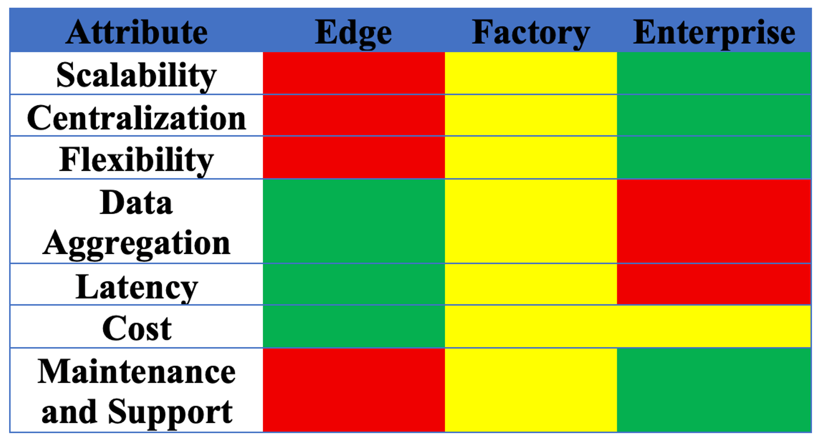
Table 1: Pros and cons of different deployment options. Green is good, yellow is okay, red is poor. Source: PDF Solutions
In the cloud
For difficult image analysis challenges, defect detectability significantly improves with advanced ML algorithms. ML model development requires hundreds of thousands of relevant images, and this is where cloud computing really shines, offering efficient GPU-based computing for processing massive volumes of data.
There is also a growing trend to combine inspection and metrology data with data collected upstream and downstream, then use it to unveil subtle defects. This pushes more computing to the cloud, illustrating the need for data infrastructure platforms that draw from multiple data sources. Here, data quality is paramount.
“ML-based inspection relies on pre-trained defect models stored in a library to recognize defects. Unlike traditional methods that depend on pattern repetition, ML algorithms analyze features from a diverse set of training images, making them well-suited for inspecting partial dies and wafer edges,” noted Woo Young Han, product marketing director at Onto Innovation. “Additionally, because ML models are trained to recognize specific defect types, defect classification occurs simultaneously with the inspection process, improving efficiency and accuracy.”
Assembling all the necessary images to build advanced ML presents a daunting investment for cost-conscious manufacturing facilities. And the complexity of the data infrastructure only grows with chiplet-based products, which source die from multiple fabs.
“The biggest hurdle preventing the customer adopting AI nowadays is the upfront cost,” said Nordson’s Zhu. “I’m not talking about the monetary cost, but about the effort to collect all the data. You need a huge amount of data to train these models. Some models require hundreds of thousands, or up to millions of image pieces. We are solving this problem by providing a generic model. We do the heavy lifting by training a model on the data we have available. But not all the model development can be done this way. It depends upon the application. For instance, we found that all the PCBs look similar in terms of component types. There is a limited number of package types (e.g. QFPs, QFNs) used per the IPC standards. We collect all these PCB component image data and train a generic model which can do segmentation on any PCB board.” [1]
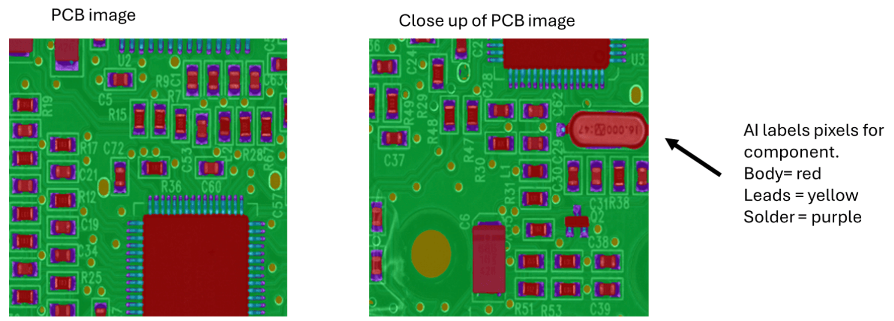
Fig. 1: AOI PCB segmentation using AI to segment/label features in AOI image. Source: Nordson Test and Inspection
Combining inspection image data with electrical test data has become standard practice in model building. This additional information provides model input to discern nuisance from impactful defects.
“Take a simple task of image classification,” said PDF’s Zamek. “For model training, one may use electrical test as the ‘ground-truth’ of whether the defect is a killer or a nuisance. To do so, one needs to gather electrical test data from a variety of steps, including wafer sort, package-level test, burn-in, and so on. And these data have to be gathered from multiple sites, ideally in a cloud for ease of use. Training requires large volume of images to cover different process technologies, inspection methods and equipment, inspection recipes, and many more. This necessitates access to scalable compute resources, driving toward cloud solutions again.”
Once built, the model can be applied at the point of inspection on an edge computer. However, continuous improvement is required. The model needs an occasional update based on data from multiple inspection/metrology tools, often from multiple manufacturing facilities. That data is fed back to the cloud, the model is modified, and then it’s deployed in tools in the field.
Connecting more data
With the ability to draw data from multiple sources, engineering teams can develop advanced ML models to uncover relationships between equipment parameters upstream, and image data and electrical test data downstream. This can identify abnormalities and speed root-cause analysis within a factory.
“The key challenge for inline metrology and inspection (in fab and foundry) is that the models trained and deployed on the equipment are limited to the data types available on that equipment, which is quite limited,” observed PDF’s Zamek. “We’ve been providing a platform that enables us to bring all data from all operations, from all sites, under one roof. And we have been seeing a growing number of use cases building and deploying models to correlate metrology to PCM, inline inspection to yield, and so on.”
Fig. 2: Typical manufacturing data pipelines that feed into the cloud for building models across factories. Source: PDF Solutions
Put simply, combining data from multiple sources within a factory and across factories has proven benefits.
“Fundamentally, data analytics approaches have evolved significantly with the onset of AI and machine learning models,” said Melvin Lee Wei Heng, director of field applications for enterprise software at Onto Innovation. “These models have greatly enhanced traceability, making it a crucial aspect of macro-defect detection and corrective actions. The ability to link and connect information from back-end to front-end processes has enabled factories to implement predictive models at the front end, even before parts arrive at the back-end process. This integration has improved response times and decision-making accuracy, leading to more efficient and effective defect management.”
At the edge
Models are built on the cloud and applied at the edge. Moving data from inspection/metrology systems to the cloud to make a decision to execute back at the system is simply impractical. For quick corrective action, inspection and metrology decisions need to be connected with upstream process data as close to real-time as possible.
“There’s always a need for rapid decision-making on inspection and metrology data, closing the loop quickly to pinpoint which process step is driving defects, determine if rework is required, and assess the impact on current WIP,” said yieldWerx’s Aslam. “The concern with relying solely on the cloud is clear — security, network latency, and potential inaccessibility. If data becomes unavailable, lots and equipment may be forced on hold until access is restored, often at a significant cost.”
Just as test systems have added a computing box alongside the ATE, inspection and metrology equipment vendors now provide a separate and local GPU computing resource.
“To maintain high throughput, ML-based inspection requires a separate graphics processing unit (GPU), which operates in parallel with conventional inspection techniques,” said Onto’s Han. “This parallel processing approach ensures that the use of ML does not negatively impact throughput while enhancing defect detection and classification capabilities.”
GPUs have simply become a necessity to support localized decision-making. “Within our product portfolios, AI has shifted workloads associated with image processing and data extraction to GPUs, enhancing the efficiency and performance of image computers,” said the KLA spokesperson. “These GPU-based image computer architectures are ‘edge’ compute systems supporting real-time data processing and the use of AI algorithms that produce instantly accessible data streams for inline monitoring, benefitting semiconductor manufacturers’ time-to-results and yield entitlement.”
Conclusion
Successfully applying AI/ML for inspection applications requires both cloud and edge computing resources and accumulated images. For model building, the cloud uses at least 100,000 images, and more often a million.
The trend to combine inspection data with other equipment data throughout the manufacturing process (e.g., electrical test) necessitates a centralized data lake that can use scalable cloud compute resources. The resulting AI/ML model improves the detection of impactful defects. Subsequently, the inspection system deploys the model at the edge with nearby GPU resources that can feed into a factory’s yield management systems.
The positive impact on yield and quality improvement in manufacturing facilities is unquestioned. “Ultimately, ML-driven analysis techniques for metrology and inspection will always vary greatly at the measurement level,” said Sean King, principal product manager at Onto Innovation. “However, as process complexity and data volumes skyrocket, using AI and ML to discern patterns and more intelligently analyze results in context becomes more common between the methods. Yield becomes less about atomized optimization of defects and process steps, and more about the holistic ‘yield space’ of intertwined (and not always clearly correlated) factors.”
Reference
https://www.electronics.org/ipc-standards, note IPC is now Global Electronics Association
Related Reading
AI/ML Challenges In Test and Metrology
New tools are changing the game, but it will take time and collaboration for them to achieve their full potential.
Metrology Under Pressure: Detecting Defects in Fine-Pitch Hybrid Bonding
Shrinking interconnects expose limitations in traditional inspection methods, forcing new approaches to overlay, surface quality, and defect detection.