
Device fabrication
We fabricated our devices using procedures similar to those described in ref. 22. A free-standing silicon nitride (SiN) membrane was used as a substrate for our van der Waals assembly that involved four atomically flat crystals (Extended Data Fig. 1). We started with etching a rectangular aperture of approximately 3 × 20 μm2 in the SiN membrane. This aperture was required to later serve as a water inlet from a reservoir placed at the back of the wafer. Using the dry transfer method, we transferred a graphite crystal (thickness approximately 10 nm) to seal the aperture. The graphite later served as the bottom electrode. It was etched through from the back side using reactive ion etching, which projected the aperture into graphite. Then a relatively thick hBN crystal (H ≈ 50–200 nm, to serve as the bottom layer) was transferred on top of the graphite and again dry-etched through from the back. Next we selected a second hBN crystal (thickness h ≈ 1–60 nm), referred to as spacer, and patterned it into parallel stripes (spaced by about 200 nm) using electron-beam lithography and reactive ion etching. We transferred the spacer layer on top of the bottom hBN using wet transfer procedures and aligning the stripes perpendicular to the rectangular aperture. Finally, the third hBN crystal was transferred on top of the spacer layer using the dry transfer method. This sealed the nanochannels as well as the aperture. The thickness of the top hBN (Htop ≈ 20–80 nm) was carefully chosen to bring the AFM tip as close as possible to the water but also to ensure that the top layer exhibits some sagging into empty channels without blocking them completely22 (Extended Data Fig. 2a,d). After each transfer, we annealed the assembly in Ar/H2 at 300 °C for 3 h and then at 400 °C for 5 h to remove polymer residues and other contamination. As the final step, we made an electrical contact with the graphite using photolithography or, alternatively, using silver paint to minimize the number of cleanroom processes. Because the top layer became flattened (no longer sagged)22 after liquid water filled the channels (see Extended Data Fig. 2d–g), this allowed us to ensure that, irrespective of the dielectric response of water, the investigated nanochannels were fully filled with water (by comparing AFM topography images before and after filling; Extended Data Fig. 2e,f). Note that, given the large in-plane conductivity of water found in this work for all thicknesses of channel, we could also verify the water filling by taking atomic force microscopy (AFM) images in the intermittent-contact attractive mode using low-f applied voltages (several kHz down to DC). In this case, the acquired contrast over the channels reversed from negative to positive on filling the water (Extended Data Fig. 2b,c) owing to the onset of strong electrostatic forces associated with the conductivity of water, as the AFM feedback adjusted the z-scanner to compensate for these forces during the scan. We emphasize that the contrast appearing in Extended Data Fig. 2c (showing roughness of several nanometres) reflects differences in the electrical properties of water and hBN (hence the red/blue colour scale) and not the actual topography, which is shown separately in grey in Extended Data Fig. 2a. When water filled the channels, the sagging disappeared and the surface became atomically flat with residual roughness of less than 3 Å independently of the channel thickness, as described previously22. This flattening is demonstrated here using true topography images in Extended Data Fig. 2e,f and their profiles (Extended Data Fig. 2g).
As another improvement with respect to our previous studies, before filling with water, we normally exposed the bottom side of the devices to low-power Ar/O2 plasma (8 W, 16 sccm Ar and 8 sccm O2 flow) for 1 s. This made SiN more hydrophilic and also cleared the entrances of channels from possible contamination. This procedure has proved beneficial for getting water inside. We also found that our devices tended to delaminate if contamination remained trapped between van der Waals layers. To prevent this from happening, great care was taken to check for cleanliness of the devices at each fabrication step (using optical and AFM imaging). For example, if dark-field optical images showed bubbles trapped between layers, such devices were discarded. Representative optical images of the studied devices with clean interfaces are provided in Extended Data Fig. 1a–c.
Local broadband dielectric imaging and spectroscopy
All SDM10,41 measurements were carried out using a commercial atomic force microscope (Nanotec Electronica with WSxM software42) operated at RT in dry atmosphere. SDM was implemented in the amplitude-modulated electrostatic-force detection mode43,44, adapting the approach described in ref. 10. Briefly, we applied an AC voltage between the AFM tip and the bottom electrode. By detecting mechanical oscillations of the cantilever, we measured the electrostatic force and, therefore, the first derivative of the tip–sample capacitance, dC/dz. Its value depends on both dielectric and conductive properties of investigated samples. SDM has previously been used for local measurements of both surface and sub-surface dielectric properties of various materials in different frequency regimes, from quasi-static to GHz (refs. 45,46,47,48). The same approach has also been widely used to study near-surface electron transport in solid samples49,50,51,52, showing the sensitivity of the technique to local conductivity. The force-sensing approach was preferable in our case to the other current-sensing and microwave-sensing AFM techniques that can also examine local impedance53,54 because the latter are generally less sensitive and more complex to implement.
To carry out dielectric spectroscopy over the required very wide bandwidth (100 Hz to 1 GHz), we combined two previously reported force-sensing detection methods. Both were implemented here using conductive diamond-coated AFM probes (CDT-CONTR or CDT-FMR from Nanosensors) with spring constant k of several Nm−1 and resonance frequency in the range 20–60 kHz. At low f up to the cantilever resonance frequency, we used the 2ω-detection approach, as described in ref. 22 for measurements of the ε⊥ of water, in which ω = 2πf is the angular frequency. Briefly, we applied an AC voltage with amplitude vAC = 4 V and measured the amplitude D2ω(z) of the resulting mechanical oscillations of the cantilever at double the applied frequency, using an external lock-in amplifier (Zurich Instruments HF2LI). The AFM tip–sample capacitance gradient was calculated as |dC/dz| = D2ω(z)4k/vAC2. Despite the relatively large AC excitation, the response remained within the linear regime, as verified by systematic amplitude-dependence measurements on reference samples and validated using relatively thick channels that exhibited the expected bulk water properties. For f higher than the cantilever resonance frequency, we used the heterodyne detection technique demonstrated in ref. 55. To this end, we applied a high-f (carrier) signal modulated by low frequency (fmod = 1 kHz, amplitude vAC = 0.5 V) using an external RF/GHz signal generator (Rohde & Schwarz SMA100B). We detected the cantilever mechanical oscillations at fmod using our external lock-in amplifier and, from those measurements, obtained the capacitance gradient at the carrier f as |dC/dz| = Dmod(z)8k/(gvAC2), in which g is the f-dependent gain of the external circuit and Dmod(z) is the amplitude of the cantilever mechanical oscillations at fmod. This approach allowed retrieval of |dC/dz| variations at f higher than the cantilever resonance frequency and up to GHz frequencies51. Note that such measurements yield only the amplitude of dC/dz and not its phase, so the obtained spectra reflect the modulus of the complex dielectric constant (see the ‘Analysis of local dielectric spectra’ section).
To minimize systematic errors, we carefully calibrated the electrical gain g for each device and atomic force microscopy tip at each measurement frequency. This is essential at high frequencies (> 1 MHz), at which both applied and measured signals show strong f-dependent variations because the cable impedance is not matched to the local sample impedance and the long-range impedance between the AFM tip and the sample. We used a calibration procedure similar to that in ref. 47, which relies on acquiring |dC/dz| curves as a function of the tip–surface distance z over a device region with f-independent impedance. We determined g by comparing |dC/dz|(z) curves at each frequency against a low-f reference curve (2 kHz), for which no gain or loss is expected. To avoid potential changes in g in different regions of the device, these curves were taken over the hBN spacer near the water-filled channel (Extended Data Fig. 3a). We then scaled them to match the 2-kHz curve using g and the offset as the two fitting parameters (Extended Data Fig. 3c). Note that, irrespective of f, the offset is always present in dC/dz curves and is typically subtracted before analysis, because it is independent of local electrical properties (see, for example, refs. 10,56). We found that, at high f (10 MHz to 1 GHz), the offsets changed substantially but were identical above water channels and hBN spacers. This confirmed that, for all of the frequencies, the offsets originated from long-range impedance contributions. Notably, although g is critical for accurately evaluating the electrical properties of water from the measured signals, offsets play little role in this study because we analysed the relative changes in |dC/dz| along the device surface–water channels versus hBN spacers (see the ‘Dielectric images and dielectric spectra acquisition’ and ‘Numerical modelling and data analysis’ sections). We validated the calibration using reference samples (hBN on doped Si), obtaining the expected f-independent dielectric spectra up to GHz frequencies (Extended Data Fig. 3e,f). Furthermore, large channels filled with water effectively served as another reference, yielding the expected spectral behaviour (flat response at high f) and the dielectric constant of bulk water. To prevent electrostatic crosstalk in calibration curves taken above hBN spacers from water inside the channels, we used channels separated by about 800 nm, a spacing chosen to be sufficiently large. Numerical simulations confirmed that, within our experimental accuracy (roughly 1 zF nm−1), the calibration curves were unaffected by electrostatics from water in the channels (Extended Data Figs. 5b and 7f). We emphasize that, if the separation were too small, such crosstalk could lead to underestimation of the dielectric constant of water.
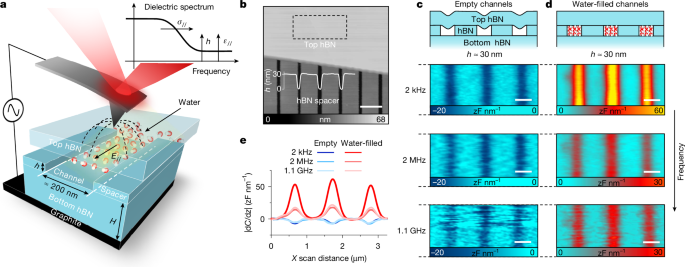
Dielectric images and dielectric spectra acquisition
The dielectric images in Fig. 1 and Extended Data Fig. 4 were taken at constant height zscan (typically about 15–25 nm) from the top layer, as in ref. 22, using the constant-height dual-pass mode SDM developed earlier10,41. In this mode, the first pass records the topography without applied voltage and the second pass acquires the dielectric image with the AFM feedback loop disabled and the z-scanner fixed (the scanner was carefully aligned parallel to the sample plane so that zscan remained constant along the horizontal direction). To avoid piezo creep effects, we allowed sufficient settling time at the beginning of each line for the scanner to reach the target height. This approach ensures maximum control of zscan, as this is measured with sub-nanometre accuracy by acquiring DC and AC deflection approach curves at scan line edges (here over the hBN spacer regions)10. The DC deflection curve allows measuring the tip–surface distance z with sub-nanometre accuracy, whereas the AC deflection curve provides |dC/dz| as a function of z, allowing further validation of zscan and correction of z-scanner drifts by matching with the |dC/dz| scan line (Extended Data Fig. 3b,c). Because the second-pass scan maintains the z-scanner fixed, potential artefacts from the z-scanner motion that would arise in the standard dual-pass ‘lift’ mode are avoided. Small variations in zscan owing to the DC electrostatic force are also measured and taken into account by recording the DC deflection during the second pass. The images as a function of f reported in Fig. 2b were taken at both constant zscan and constant y position (y-axis is along the nanochannels length). We typically recorded 25 lines at each f. Standard AFM image processing consisting of flattening and Gaussian filtering was applied.
The dielectric spectra in Fig. 2a and Extended Data Fig. 10 were obtained for constant zscan (about 15–20 nm) and constant y but after acquiring the entire 3D dataset |dC/dz|(x,z,f), such as that shown in Extended Data Fig. 3d. This set is composed of many |dC/dz|(x,z) images (Extended Data Fig. 3a), which were obtained at different f by scanning the AFM tip across the channels (along the x-axis) at constant y and approaching the surface in steps. This refined procedure was necessary here to minimize errors in zscan owing to z-scanner drifts during long measurements across the whole frequency sweep. Although the spectral behaviour does not change with scan height, the amplitude of |dC/dz| does (Extended Data Fig. 6g,h), making it essential to maintain the same zscan at each f for high accuracy in our spectral analysis. When taking |dC/dz|(x,z) images, the AFM tip was approached from larger distances towards the surface down to the minimum distance of typically about 15 nm, beyond which tip collapse occurred owing to long-range attractive electrostatic forces, as expected under our measurement conditions (applied voltage, RT, soft cantilevers and large AFM tip radii). At each step, we acquired dozens of lines, which were then averaged to obtain the corresponding profile (Extended Data Fig. 3b). This notably improved the signal-to-noise ratio. By taking small steps towards the surface, we could then reconstruct the dielectric spectra (Extended Data Fig. 10) by using the value measured in the middle of nanochannels at the same zscan (±1 nm) for each f. This 1-nm uncertainty has negligible impact on the extracted electrical properties shown in Fig. 3, as demonstrated in Extended Data Fig. 7g,h (see also the ‘Numerical modelling and data analysis’ section). We note that all of the spectra were obtained at the nearest possible distances achievable before tip collapse to ensure maximum signal strength and measurement stability. Larger zscan were avoided, as the |dC/dz| signal decays rapidly with z, compromising measurement accuracy, particularly for small channels (Extended Data Fig. 6g,h).
As well as the scanning height zscan, the spectral values depended on geometry/size of our devices and the AFM tip parameters (Extended Data Fig. 10). All of the necessary geometric parameters of the studied devices were measured by taking their topography images, whereas the AFM tip parameters (its radius R and half-angle θ) were determined by fitting |dC/dz|(z) curves taken directly above the graphite bottom layer, as in ref. 22, following the procedures described in refs. 56,57. For example, the tip radii were found to be in the range 50–200 nm, in good agreement with the values specified for commercial diamond-coated tips. This enabled quantitative analysis of the ‘absolute-value’ spectra (shown in Extended Data Fig. 10) as opposed to just relative variations with f, through full-3D numerical simulations that account for the detailed geometry of the system (see the ‘Numerical modelling and data analysis’ section). We emphasize that the values of |dC/dz| in the spectra that we analysed to extract the electrical parameters of water are the peak values over the centre of the water channel relative to the values measured over the centre of the hBN spacers at the same scan height, as in ref. 22. This differential approach makes our analysis robust against uncertainties in geometric parameters and eliminates the influence of the long-range geometry of the system, as described below.
To facilitate direct comparison of the electrical response of water across different devices and experiments and enhance clarity of presentation, we normalized our representative spectra for various water thicknesses in Fig. 2a. This normalization used the low-f plateau as a reference point, dividing each spectrum by this value. In this low-f regime, the measured signal becomes effectively independent of both the electrical properties of water and its thickness (see Extended Data Figs. 6b and 8b and the ‘Analysis of local dielectric spectra’ section). As the signal in this regime is primarily determined by the AFM tip radius and its distance from the channel, normalizing with respect to the low-f value effectively eliminates the geometric contributions, allowing for more direct comparison between different experiments. We emphasize that alternative normalization using high-f values would not be beneficial, as the signal in this regime strongly depends on both the channel thickness and its dielectric properties.
Numerical modelling and data analysis
The observed dielectric spectra were fitted to full-3D finite-element numerical calculations implemented using COMSOL Multiphysics 5.4a (AC/DC electrostatic module), not other simplified models presented in the manuscript. These 3D calculations were based on the electrostatic model previously used in ref. 22, adapted here to simulate the frequency-dependent force acting on the tip as a function of ε and σ of water when an AC electric field was applied. They compute absolute |dC/dz| values while fully accounting for the actual geometry and dimensions of the system, including the tip and device, as well as the conductive and dielectric properties of water and their anisotropy, thereby eliminating potential geometric and electrostatic artefacts that could arise in the data analysis using simplified models.
A schematic of the model is shown in Extended Data Fig. 5a. Following ref. 22, the AFM tip was modelled as a truncated cone with the half-angle θ terminated with a tangent hemispherical apex of radius R. The values of θ and R used in our simulations were measured for each AFM tip, as discussed above. The AFM cone height Hcone was limited to 6 μm and the cantilever was omitted to reduce the computational time (unless stated otherwise). We checked that these approximations had no impact on the simulated results. The simulated nanochannel consisted of two insulating slabs of hBN separated by a lossy water slab of height h and width w (measured from topography for each device). We modelled each slab explicitly with its own respective dielectric constant and conductivity according to the general definition of anisotropic, complex dielectric constant
$${\varepsilon }_{\perp ,//}^{* }(\omega )={\varepsilon }_{0}{\varepsilon }_{\perp ,//}-{\rm{i}}\frac{{\sigma }_{\perp ,//}}{\omega },$$
(1)
in which ω is the angular frequency, ε0 is the dielectric permittivity of vacuum, ε⊥ and ε// are the dielectric constants perpendicular and parallel to the channel, respectively, and σ⊥ and σ// are the corresponding conductivities, respectively. Note that, for the water slab, the imaginary term in equation (1), represented by σ⊥,//, accounts for all possible losses, including those from charge transport and dipolar relaxation, whereas ε⊥,// may contain ionic contributions owing to ion–water and ion–ion correlations, as well as the purely dielectric response of water58,59. Both ε⊥,// and σ⊥,// of water were treated here as frequency-independent, as this approximation adequately reproduces the observed dispersion, as explained below and also in the ‘Analysis of local dielectric spectra’ section. For hBN, σ⊥,// is zero, so its \({\varepsilon }_{\perp ,//}^{* }\) reduces to its known real part, ε⊥hBN = 3.5 and ε//hBN = 5.5, which are constant within our experimental bandwidth. To model possible contributions from nearby nanochannels, the device was modelled as three parallel water nanochannels of length l = 3 μm and measured spacing ws within the surrounding hBN dielectric matrix, with dimensions matching the measured top, bottom and spacer hBN layers (length l = 3 μm, width W = 3 μm and height Htop + h + H).
We numerically solved the Poisson’s equation in the frequency domain for each device, calculated the force acting on the AFM probe and, from that, obtained |dC/dz| by integrating the built-in Maxwell stress tensor on the surface of the probe. The simulations used the same box size and boundary conditions as in ref. 22. Examples of calculated dielectric spectra for representative geometrical parameters of our devices and ε and σ of water are shown in Extended Data Fig. 6. These simulations closely match the experimental spectra, reproducing the observed Debye-type frequency dispersion.
Our modelling approach is equivalent to the original analysis by Maxwell and Wagner60,61, which led to the Debye-like Maxwell–Wagner (MW) formalism commonly used to interpret dielectric relaxations arising from DC conductivity in macroscale spectra of heterogeneous lossy dielectrics62,63,64 (see the ‘Alternative phenomenological Debye-like MW analysis’ section). Using the complex dielectric constants defined in equation (1), Maxwell and Wagner showed that the effective capacitance of a planar layered system, in which each layer has constant ε and σ, acquired a frequency dependence similar to a Debye-type relaxation62,63. In our case, the AFM tip replaces the top electrode in their derivation, precluding an exact analytical solution and necessitating 3D numerical simulations. Nevertheless, the underlying electrostatic problem is the same, therefore no further frequency dependence of ε and σ in equation (1) for the water slab is required to reproduce the observed dispersion, unless an extra relaxation process is present. In our case, no such further relaxation needs to be assumed or is expected to occur, based on present understanding of strongly confined water. Consistent with this, the experimental spectra exhibited only a single Debye-like relaxation at lower frequencies arising from DC conductivity (for more details, see the ‘Analysis of local dielectric spectra’ section).
Experimental |dC/dz| spectra were fitted with the ε// and σ// of water as the only fitting parameters. All of the other parameters needed for the simulations were determined experimentally, as detailed above. ε⊥ was set to the values measured in ref. 22 and σ⊥ was set to the measured value for our bulk water (σbulk = 2 × 10⁻⁴ S m−1). The extracted ε// and σ// values were found to depend little on exact values of ε⊥ or σ⊥, indicating that our experimental geometry was rather insensitive to the out-of-plane characteristics of water, and the influence was negligible for our smallest channels (Extended Data Figs. 6e,f and 8e,f). This is because the impedance of the nanochannel in the out-of-plane direction is much smaller than the series impedance from the hBN layers and AFM tip–surface capacitances, whereas the impedance of the nanochannel in the in-plane direction is much larger (see the ‘Electrical modelling’ section). From these fitted values of ε// and σ//, we inferred the interfacial dielectric constant, ε//int, and conductivity, σ//int, of the confined water layer using the three-capacitor model, as explained in the main text, without introducing ε//int and σ//int directly into the electrostatic problem. This approach minimized the complexity of our numerical calculations.
For brevity, in all of the figures, |dC/dz| refers to the relative dielectric contrast (unless stated otherwise), that is, the response relative to the hBN spacer so that |dC/dz| ≡ dC(zscan,ε⊥,//,σ⊥,//)/dz − dC(zscan,ε⊥,//hBN,0)/dz. Accordingly, we computed the absolute value of |dC/dz| over the centre of the water channel as a function of f and subtracted the corresponding values for the case of the tip placed over the centre of the hBN spacer, matching the experimental data processing. This differential approach avoids systematic errors. As mentioned above, it reduces the impact of uncertainties in geometric parameters and allows us to model only the local geometry, as the long-range geometric contributions do not affect |dC/dz| variations relative to the spacer. Furthermore, each device was modelled using its actual dimensions (spacer and channel width and height, top and bottom hBN heights) and with the measured radius of the AFM tip used in that experiment. This ensured that the 3D calculations reproduced the realistic electric-field distribution between the tip and the confined water, yielding reliable electrical properties of water with minimal approximations.
The thickness H of the hBN bottom layer determines whether the measurements are mostly sensitive to ε// or ε⊥. Extended Data Fig. 7 illustrates this for the case of channel thickness h = 5 nm at high f, beyond the conductivity relaxation regime (see the ‘Analysis of local dielectric spectra’ section) and for a large AFM tip radius (100 nm), as used in our experiments. When the channel is in the immediate proximity to a metallic surface (Extended Data Fig. 7a), as in ref. 22, the |dC/dz| signal is independent of ε// and, consequently, the extracted ε represents the out-of-plane component, ε⊥. Furthermore, measurements are sensitive only to relatively small values of ε⊥ (up to about 20 for h = 5 nm), as the signal saturates with further increases in ε⊥ (for larger channel thicknesses, the sensitivity extends to increasingly larger values of ε⊥, as shown in ref. 22). Conversely, when the channel is on a thick hBN layer (H = 200 nm; Extended Data Fig. 7b), the |dC/dz| signal greatly increases for ε// > 20, becoming dominated by the in-plane component. Therefore, for relatively large values of ε// ranging from about 80 to about 1,000, as measured in this work, the signal at such H shows little dependence on ε⊥. Extended Data Fig. 7c shows how the signal evolves as a function of H. In these simulations, we increased the cone height and cantilever length of the AFM tip to their nominal values (Hcone = 12 μm and Lcantilever = 20 μm). This allowed us to include electrostatic contributions from longer-range components of the atomic force microscopy probe65, which we found to be relatively small but still non-negligible for very thick bottom hBN (H > 500 nm). The results show that the |dC/dz| signal and its sensitivity to ε// peaks between 50 and 500 nm (Extended Data Fig. 7c). For thinner hBN layers, the ε// contribution is relatively small or negligible and the signal is dominated by ε⊥. For hBN thicker than 500 nm, the |dC/dz| signal decreases, becoming less sensitive to the investigated local electrical properties, consistent with previous results56. This is expected because the AFM tip is moved far away from the bottom electrode. In this work, we used bottom hBN layers of thickness up to 200 nm. This limitation was dictated by constraints in the fabrication of our devices, because thicker hBN crystals were stiffer and provided poor adhesion, leading to delamination on filling the channels with water.
We emphasize that, because the amplitude of the dielectric spectra depends on the scan height, data analysis may also be affected by this parameter. Specifically, although the value of σ// is independent of zscan (as the cut-off frequency remains unchanged with scan height; Extended Data Fig. 6g,h), the extracted ε// may be influenced, as it is given by the amplitude of the high-f plateau. As described above, in this study, we used special procedures to control zscan and determine its value with maximum possible accuracy, estimated at ±1 nm. Despite the steep increase of |dC/dz| with decreasing z, such 1-nm experimental uncertainty has negligible impact on the extracted ε//, even for our smallest channels. This is because our analysis relies on the measurement of variations of |dC/dz| relative to the hBN spacer region at the same zscan. This differential approach makes the analysis robust against small uncertainties in zscan. To illustrate this robustness, Extended Data Fig. 7h shows 3D simulated curves for the best-fit zscan value (corresponding to the data in Extended Data Fig. 10c) and for best-fit zscan ± 1 nm. The three curves nearly overlap, with experimental data points scattered around them, consistent with the stated ±1 nm experimental uncertainty. The obtained 30% error in the extracted ε// = 900 incorporates this uncertainty, along with the standard deviation for data points on the high-f plateau. Notably, qualitative experimental evidence allows us to discard large uncertainties in zscan as an alternative explanation for the enhanced ε// observed in our smallest water channels. Indeed, to justify the large values of |dC/dz| observed at high f with bulk-like ε// would imply extremely small scan heights (⪝5 nm). This is shown in Extended Data Fig. 7g, in which we plot the sensitivity curve of |dC/dz| to ε// at various values of zscan for 1.5-nm channels. However, such small values of zscan are physically impossible in our constant-height scan mode, as below about 15 nm, the tip collapses onto the surface (see the ‘Dielectric images and dielectric spectra acquisition’ section). Also, the implied small values of zscan would lead to much larger |dC/dz| values than observed for the low-f spectral plateau, which is highly sensitive to the scan height (see the ‘Analysis of local dielectric spectra’ section). In other words, although the high-f plateau could theoretically be reproduced by assuming a much smaller scan height (roughly 5 nm for the case of the representative device with h ≈ 1.5 nm in Extended Data Fig. 10c), such a simulation would fail to reproduce the low-f plateau, as shown in Extended Data Fig. 7h. These observations rule out substantial errors in zscan and the large ε// reported here for our smallest devices can be explained by inaccuracies in the scan height.
We stress that the electric field above the hBN spacer varies little with the electrical properties of confined water (Extended Data Fig. 5c–h) and that our differential analysis relative to the hBN spacer region does not introduce systematic errors associated to such electric-field variations. This is demonstrated in Extended Data Fig. 5b, which shows full-3D numerical simulations of the absolute value of |dC/dz| versus tip-surface distance z calculated with the tip above the centre of the hBN spacer at different f, comparing water-filled and empty channels, for our smallest channels (h = 1.5 nm). All curves practically overlap, with deviations at intermediate and high f not exceeding 0.1 zF nm−1, an order of magnitude smaller than our experimental uncertainty (about 1 zF nm−1). Only at the lowest f do the deviations increase notably because of the in-plane conductivity of water but still remain within experimental uncertainty. Furthermore, despite their minimal impact, these small variations are fully accounted for in our analysis, which incorporates the realistic electric-field distribution and device geometry. This also shows that, even if these field variations were not accounted for—for example, if using the simplified analytical model described below—the errors would be negligible, particularly at GHz frequencies at which we extract ε//.
Analytical modelling
Because of the non-uniform distribution of electric field across nanochannels and the complex geometry of AFM probes, the electrostatic problem cannot be solved exactly using analytical models. Hence, to fit the experimental data and obtain the results shown in Fig. 3, we used the 3D numerical simulations described above. Nonetheless, it is informative to provide an analytical approximation that would substantiate our numerical results and offer further physical insight into the observed spectral behaviour that is relatively independent of the details of experimental geometry. Such an approximation could be used for semi-quantitative estimates. To this end, we used the point-charge model in which the AFM tip was replaced by a point charge Q positioned at distance z = zscan + R from the top hBN surface (Extended Data Fig. 8a). The devices were modelled as a stack of different slabs, infinite in the in-plane direction. The slabs corresponding to the hBN layers were positioned at 0 < z < −Htop and −(Htop + h) < z < −(Htop + h + H) and modelled as insulators with zero conductivity. The water layer at −Htop < z < −(Htop + h) was described by anisotropic dielectric constants ε//,⊥ and conductivities σ//,⊥. The boundary condition of zero voltage was imposed at z = −(Htop + h + H) to model the highly conducting ground electrode. By making use of the in-plane translational invariance, the Laplace equation for the Fourier transform electrostatic potential in the in-plane direction ϕq(z) becomes
$${q}^{2}{\varepsilon }_{//}(z){\phi }_{q}(z)-{\partial }_{z}({\varepsilon }_{\perp }(z){\partial }_{z}{\phi }_{q}(z))={Q}_{q}\delta (z-{z}_{{\rm{scan}}}-R)$$
(2)
in which q = (qx,qy) is the wave vector in the in-plane direction and the position-dependent dielectric constants are denoted as ε//(z) and ε⊥(z), respectively. The dielectric constant of the hBN slabs was, for simplicity, assumed to be isotropic with ε//(z) = ε⊥(z) = εhBN = 4. The Laplace equation was solved within each slab using exponential functions. The solutions were matched at each interface by imposing the following boundary conditions: continuity of ϕq(z) and
$${\varepsilon }_{\perp }(z+\eta ){\partial }_{z}{\phi }_{q}(z+\eta )-{\varepsilon }_{\perp }(z-\eta ){\partial }_{z}{\phi }_{q}(z-\eta )=0$$
(3)
in which η is an infinitesimal constant. A similar relation holds at the point-charge location, zscan + R, but the right-hand side in equation (3) becomes equal to Q. The potential in real space ϕ(r,z) was then obtained by performing the Fourier transform of ϕq(z) in the in-plane direction. The capacitance was estimated as C = Q/ϕ(0,zscan) and, from the latter, the capacitance gradient |dC/dz| was calculated. Examples of the calculated dielectric spectra for representative parameters of our devices and ε and σ of water are given in Extended Data Fig. 8, in which, again for brevity, |dC/dz| indicates its value relative to the case of the heterostructure fully made of hBN, |dC/dz| = dC(zscan,ε⊥,//,σ⊥,//)/dz − dC(zscan,εhBN,0)/dz. The calculated spectra show that the model captures all of the main features of the observed behaviour as a function of various parameters and agrees well with our numerical simulations in Extended Data Fig. 6. Note, however, that, because the analytical model assumes an infinite water layer and does not account for a finite w, the transition between low-f and high-f plateaus becomes less pronounced (Extended Data Fig. 8d). The analytical results agree with the numerical simulations only for w much larger than the tip radius R (Extended Data Fig. 6d). Accordingly, if only the analytical model were used to fit the reported experimental data, this would result in systematic underestimation of both ε// and σ//. In particular, the values extracted for quasi-2D water layers (h ⪝ 2 nm) would be underestimated by a factor of about 5, although all of the trends with changing h would remain correct.
Analysis of local dielectric spectra
The observed dispersion arises from DC conductive losses of water within the channels, not from its dipolar orientational (Debye) relaxation66. The latter in bulk water occurs only at f ≈ 10 GHz (ref. 67), well above the frequencies examined here. Furthermore, the spectra exhibit very high low-f plateaus, which, if fitted with Debye-like models, would yield physically implausible values for the ε// of water (see the ‘Alternative phenomenological Debye-like MW analysis’ section). Instead, these plateaus are accurately reproduced by our model using realistic values of σ// of water in the conductive term of equation (1). A similar situation is encountered in the analysis of macroscale dielectric spectra of heterogeneous lossy dielectrics measured by broadband dielectric spectroscopy62 (for example, colloidal suspensions and composite liquid/solid materials such as water confined in porous media68,69), in which MW interfacial polarization relaxations60,61 emerge. In such complex heterogeneous systems, phenomenological Debye-like models become necessary, because the measured response represents the effective dielectric constant of the entire system and explicit modelling of each dielectric component is precluded by geometric complexity. Although these approximations can fit macroscale spectra, they typically yield unrealistically high ε at low frequencies, often reaching very large values (>104). Such high apparent permittivities, also reported for water confined in porous media68, do not represent intrinsic dielectric constants but, rather, reflect DC conductive losses68,70. By contrast, our three-layer nanochannel system enables a ‘first-principles’ description in which each dielectric layer is modelled explicitly with its own frequency-independent ε and σ, as in equation (1). This approach allows ε// and σ// to be determined independently from the spectra without introducing unphysical parameters or approximations.
No further frequency dependence of ε// and σ// of water was required in this analysis, as the measured spectra show only a single Debye-like relaxation at low f arising from DC conductivity, with no indication of more relaxations. This is evident from the high-f plateaus, which remain flat and correspond to bulk-like or enhanced values of ε//. If in our smallest channels (<4 nm) the intrinsic dipolar relaxation of water were shifted to lower f by the geometric confinement, we would expect either an extra dielectric plateau or broadening of the Debye-like relaxation transition region, both leading to reduced high-f values of ε//. Instead, we consistently observed high, flat plateaus at high f across all of our devices, ruling out further dipolar relaxations in the in-plane direction. The same reasoning applies to anomalous Debye-like dipolar relaxations of the hydrogen-bond network reported for confined water69 in the 100 kHz to 10 MHz range, which would also reduce both the low-f and the high-f plateaus, an effect not observed here. Although a weak dipolar relaxation from hydrogen-bond restructuring in the out-of-plane direction cannot be entirely ruled out in our largest channels, this is unlikely for our smallest channels, which show very low ε⊥ at low frequencies (kHz), as previously reported22. In any case, variations in ε⊥ have negligible impact on the extracted ε// and σ// and, therefore, would not alter our conclusions.
The reason for a DC conductivity contribution to our spectra can be understood by noticing that we measured the modulus of dC/dz, that is, the modulus of the complex dielectric constant \({|\varepsilon }_{\perp ,//}^{* }(\omega )|\). As a result, the dielectric response is determined by both ε and σ and, depending on frequency, either the first or the second term in equation (1) becomes dominant. At sufficiently low f, the conductivity term always dominates \({|\varepsilon }_{\perp ,//}^{* }(\omega )|\), similar to the case of macroscale measurements using standard broadband dielectric spectroscopy62. To this end, it is useful to recall that, at low frequencies, the spectrum of deionized water at macroscale is known67 to be dominated by σbulk. Therefore, the spectrum is effectively divided into two regions separated by the conductivity relaxation frequency, fr,bulk, at which the behaviour changes. In the conduction-dominated region (f < fr,bulk), the dielectric response decreases with increasing f, whereas for f > fr,bulk, it is constant and depends only on εbulk. The value of fr,bulk is given by62
$${f}_{{\rm{r,bulk}}}=\frac{{\sigma }_{{\rm{bulk}}}}{2{\rm{\pi }}{\varepsilon }_{0}{\varepsilon }_{{\rm{bulk}}}}$$
(4)
which follows from equation (1) if we use |ε⊥,//| = εbulk and |σ⊥,//| = σbulk. Note that this frequency is analogous to the cut-off frequency for systems that can be modelled by a simple RC circuit (see the ‘Electrical modelling’ section). For the bulk water used in our experiments (εbulk ≈ 80, σbulk ≈ 2 × 10⁻⁴ S m−1), equation (4) yields approximately 45 kHz. This value agrees well with fr,bulk obtained from both numerical and analytical modelling discussed above for the specific experimental geometry. Indeed, the analyses shown in Extended Data Figs. 6b and 8b yielded the purely dielectric behaviour characterized by high-f plateaus starting at f ⪞ 45 kHz for all of our nanochannels, irrespective of their height h. The extra plateau found in our simulations at low f reflects the presence of non-lossy dielectrics (air gap between the AFM tip and the device; the top and bottom hBN layers). These dielectrics can be represented as further capacitances in series to the contribution of water (see the ‘Electrical modelling’ section). Accordingly, for f below the cut-off frequency fc,bulk, the modelled response becomes purely dielectric, reflecting the series capacitances. For fc,bulk < f <fr,bulk, the response is dominated by the σ of water, whereas above the relaxation frequency fr,bulk, it is again purely dielectric but now dominated by the ε of water. For other relevant values of σ and ε of water, the spectra exhibit similar behaviour (Extended Data Figs. 6e,f and 8e,f): there is a low-f plateau up to the cut-off frequency fc, above which the response decreases with increasing f, and the high-f plateau develops above the conductivity relaxation frequency fr.
The onset of the low-f plateau with decreasing f is determined by the in-plane conductivity of water σ//, whereas no information can be inferred about σ⊥ from our experimental data because the measurement geometry is insensitive to the latter conductivity. This can be seen in Extended Data Figs. 6e and 8e, in which the low-f plateau shifts in frequency with varying σ//, but not σ⊥, and completely disappears if σ// = 0 and σ⊥ ≠ 0. Qualitatively, the stronger dielectric response at low f reflects the fact that the electric potential drops mostly between the AFM tip and the conductive water layer. We used our numerical simulations to illustrate this effect (Extended Data Fig. 5). At low f and σ// ≠ 0, the electric potential decreases almost entirely across the air and the top hBN layer with little voltage drop left below the water layer (Extended Data Fig. 5f). Also, the potential distribution extends along the length of the nanochannel for several micrometres (Extended Data Fig. 5d). By contrast, at high f > fr, the potential drop occurs across the entire thickness of our devices, similar to the case in which the AFM tip is placed above hBN spacers (Extended Data Fig. 5f–h). The potential drop at high f also extends nearly equally in all of the lateral directions around the tip apex (Extended Data Fig. 5e), similar to the case in Extended Data Fig. 5c for non-conducting water layer (σ// = 0). The effective screening by the conductivity of water along the channel length explains the observed large low-f response. Note that the absolute value of the low-f response is independent of σ// but depends on geometric parameters, in particular the channel width w, tip radius R (Extended Data Fig. 6c) and the bottom-layer thickness H (Extended Data Figs. 7c and 8c). This makes simulations essential for accurate evaluation of the magnitude of changes on the dispersion curves.
Although the value of σ// does not affect the low-f response, it controls the cut-off frequency fc, which shifts to higher f proportionally to σ// (Extended Data Figs. 6e and 8e) but independently of ε// (Extended Data Figs. 6f and 8f). This behaviour can be described by
$${f}_{{\rm{c}}}=\alpha \frac{{\sigma }_{//}}{2{\rm{\pi }}{\varepsilon }_{0}},$$
(5)
in which α is the geometrical parameter that can be estimated analytically (see the ‘Electrical modelling’ section). For more accurate results, α was obtained using numerical simulations (Extended Data Fig. 10), which yielded α ≈ 2.8 × 10⁻³, 6.2 × 10⁻⁴ and 9.2 × 10⁻⁵ for our three representative devices discussed in the main text, with h ≈ 30, 5 and 1.5 nm, respectively. These values of α suggest that fc should shift relatively little (from about 10 kHz to about 500 Hz) if water filling the channels exhibited the bulk properties (Extended Data Figs. 6b,c and 8b,c). This shift is much smaller than that observed experimentally and, in fact, occurs in the opposite direction, towards lower f for smaller h, in strong contrast to the experimental behaviour (Fig. 2a). This reiterates the fact that the observed increase in fc with decreasing h cannot be associated with changes in geometry but comes from a huge increase in the σ// of water for stronger confinement.
At high f, beyond the conductivity relaxation regime, water behaves as a purely dielectric media and, accordingly, the relative height of the high-f plateau is no longer dependent of σ// but depends on the ε of water, the geometry of the channel (in particular its height h) and the AFM tip radius (Extended Data Fig. 6c). The height of the plateau allows us to extract ε// using numerical simulations. Notably, for small channels and large in-plane dielectric constant (ε// ≥ 80), the contribution of ε⊥ becomes negligible (Extended Data Figs. 6f and 8f). Furthermore, we find that fr shifts to higher frequencies proportionally to σ// and inversely proportionally to ε// and is given by
$${f}_{{\rm{r}}}=\frac{{{\sigma }}_{//}}{2{\rm{\pi }}{{\varepsilon }}_{0}{{\varepsilon }}_{//}}.$$
(6)
This equation is independent of the device geometry and presents an equivalent of equation (4) valid at the macroscale. Therefore, once σ// is known, ε// can be directly obtained from fr using equation (6), provided that fr is well separated from fc, as in the case of our smallest channels. Also, if α is known, both σ// and ε// could be readily estimated from the two characteristic frequencies fc and fr without the need for simulations, simply using the equations
$${\sigma }_{//}=\frac{{2{\rm{\pi }}{\varepsilon }_{0}f}_{{\rm{c}}}}{\alpha },$$
(7)
$${\varepsilon }_{//}=\frac{{f}_{{\rm{c}}}}{\alpha {f}_{{\rm{r}}}},$$
(8)
which follow directly from equations (5) and (6). Note that the above considerations and equations (5)–(8) can also be helpful for the analysis of dielectric spectra obtained using other scanning probe approaches44, including those that examine higher derivatives of |dC/dz| and scanning impedance/microwave microscopy that directly investigates the local impedance.
Electrical modelling
It is instructive to use an equivalent impedance circuit to describe the observed dielectric dispersion. However, because of long-range contributions from various AFM cantilever components and the complex geometry of our nanochannel devices that result in a non-uniform distribution of the electric field, an equivalent circuit should be so complicated that it is unrealistic to describe our spectra quantitatively. Below, we provide a simplified model that aims to explain the physics behind and support our numerical results (Extended Data Fig. 9). To this end, the AFM tip–nanochannel interaction can be modelled by the capacitance, Ctip, that—for simplicity—accounts for both tip–air and top-hBN-layer capacitances and, to a first approximation, can be calculated as Ctip = 2πε0Rln(1 + R(1 − sinθ)/(zscan + Htop/ε⊥hBN)) using the formula described in ref. 57. We neglect the stray capacitances associated with the AFM cantilever and consider only the tip apex capacitance that is expected to provide the dominant contribution. As for the water-filled nanochannel, we consider it as a distributed RC network shown in Extended Data Fig. 9a. It consists of two elementary RC circuits describing in-plane and out-of-plane impedances Z//(ω) = R///(1 + iωR//C//) and Z⊥(ω) = R⊥/(1 + iωR⊥C⊥), respectively. R⊥,// and C⊥,// can be estimated as C// = ε0ε//wh/Δl, R// = Δl/(σ//wh) for the in-plane direction and C⊥ = ε0ε⊥wΔl/h and R⊥ = h/(σ⊥wΔl) for the out-of-plane direction, in which Δl is the length of the circuit element along the channel. We also considered another capacitance Cb in series to Z⊥, to model the effect of the bottom hBN layer between the water channel and the ground. Plugging in the experimental values relevant to our devices, we can readily find that Z⊥(ω) ≪ 1/(ωCb) for all frequencies, meaning that the contribution of Z⊥(ω) is negligible in our experiments, in agreement with the above numerical and analytical calculations. The distributed network can then be simplified further and described by the electrical circuit shown in Extended Data Fig. 9b, in which the water impedance is modelled by a single RC unit in the in-plane direction, that is, Zch(ω) = R///(1 + iωR//C//), in which C// = ε0ε//wh/l*, R// = l*/(σ//wh) and l* is the effective length of the nanochannel contributing to electrostatic interactions with the AFM tip. With reference to Extended Data Fig. 5d, l* notably exceeds the tip diameter and, without loss of generality, can be assumed to be on the order of several micrometres. The total equivalent impedance between the AFM tip and the ground is then given by
$$Z(\omega )=\frac{1+{{\rm{i}}\omega R}_{//}({C}_{//}+{C}_{{\rm{geom}}})}{{\rm{i}}\omega {C}_{{\rm{geom}}}(1+{\rm{i}}\omega {R}_{//}{C}_{//})},$$
(9)
in which Cgeom = CtipCb/(Ctip + Cb) is the capacitance that depends on geometric parameters but not on the electrical properties of water. Extended Data Fig. 9c shows |Z| as a function of f for the three representative devices. The effective capacitance of the modelled circuit is given by 1/ωZ(ω) and shows the same qualitative dependence on f, σ and ε of the capacitance gradient, |dC/dz|. Extended Data Fig. 9d plots |1/ωZ(ω)| that indeed exhibits both low-f and high-f plateaus characterized by frequencies fc and fr, in good agreement with the experiment and numerical simulations. Despite its simplicity, the electrical model also reproduces well the changes in the high-f plateau with varying ε// of water (Extended Data Fig. 9f) and changes in fc with varying σ// (Extended Data Fig. 9e).
Using this model, we can also corroborate the expressions for fc and fr given by equations (5) and (6). Indeed, the pole of equation (9) yields the relaxation frequency as fr = 1/(2πR//C//) and, plugging in R// and C// in terms of σ// and ε//, results in equation (6). The zero of equation (9) yields the cut-off frequency so that fc ≅ 1/(2πR//Cgeom), for which we take into account that Cgeom is larger than C//. Accordingly, fc is proportional to σ// ∝ 1/R// and depends on the measurement geometry (through Ctip and Cb) but is independent of ε//, in agreement with our numerical simulations. Expressing Ctip, Cb and R// in terms of geometric and electrical parameters as defined above and taking Cb = ε0εhBNwl*/H, we obtain equation (5), in which, in the case of our geometry, the geometric factor α can be approximated to α ≅ (hw/l*)(1/(2πR) + H/(εhBNwl*)). Using the specific parameters for our representative devices (h ≈ 30, 5 and 1.5 nm) and the effective channel length l* = 3 μm, this yields α of about 4 × 10⁻³, 1 × 10⁻³ and 2 × 10⁻⁴, respectively, in reasonable agreement with the numerically simulated values of α. Thus, equations (7) and (8) with α calculated analytically, as obtained from the simplified electrical model shown in Extended Data Fig. 9b, also allow for semi-quantitative estimates of σ// and ε//, which are found to differ by only a factor of less than 2 from the values extracted through our more quantitative, numerical analysis.
Alternative phenomenological Debye-like MW analysis
For completeness, we demonstrate that applying the MW formalism typically used for macroscale dielectric spectra62,63,64 would yield the same ε// and σ// values as reported in Fig. 3, although in a more convoluted way. In this alternative framework, the anisotropic, complex dielectric function in equation (1) for the water slab is replaced with the following expression:
$${\varepsilon }_{\perp ,//}^{* }(\omega )={\varepsilon }_{0}\left({\varepsilon }_{{\rm{h}}f\perp ,//}+\frac{{\varepsilon }_{{\rm{l}}f\perp ,//}-{\varepsilon }_{{\rm{h}}f\perp ,//}}{1+{\rm{i}}\omega {\tau }_{\perp ,//}}\right)-{\rm{i}}\frac{{\sigma }_{\perp ,//}}{\omega },$$
(10)
in which τ⊥ and τ// are characteristic Debye-type relaxation times and εlf⊥ (εhf⊥) and εlf// (εhf//) are the low-f (high-f) dielectric constants of the water slab, respectively, in each direction. No broadening parameters are required, as a single, ideal Debye-type relaxation describes our spectra. We omit the explicit conductivity term and further simplify equation (10) to:
$${\varepsilon }_{\perp ,//}^{* }(\omega )={\varepsilon }_{0}\left({\varepsilon }_{{\rm{h}}f\perp ,//}+\frac{{\varepsilon }_{{\rm{l}}f\perp ,//}-{\varepsilon }_{{\rm{h}}f\perp ,//}}{1+{\rm{i}}\omega {\tau }_{\perp ,//}}\right),$$
(11)
because the Debye term in equation (10) inherently accounts for conductivity contributions at finite frequencies. This is evident by rewriting equation (11) in terms of its real and imaginary parts:
$${\varepsilon }_{\perp ,//}^{* }(\omega )={\varepsilon }_{0}\left({\varepsilon }_{{\rm{h}}f\perp ,//}+\frac{{\varepsilon }_{{\rm{l}}f\perp ,//}-{\varepsilon }_{{\rm{h}}f\perp ,//}}{1+{\omega }^{2}{{\tau }_{\perp ,//}}^{2}}\right)-{\rm{i}}\left(\frac{({\varepsilon }_{{\rm{l}}f\perp ,//}-{\varepsilon }_{{\rm{h}}f\perp ,//})\omega {\tau }_{\perp ,//}}{1+{\omega }^{2}{{\tau }_{\perp ,//}}^{2}}\right).$$
(12)
This equation reproduces the observed spectral behaviour. However, because the imaginary part vanishes as ω → 0, fitting the observed low-f plateau requires assuming unrealistically large in-plane εlf//, as usually happens in the MW analysis of macroscale systems68,70. Extended Data Fig. 11 shows results from implementing equation (10) in our 3D numerical simulations and fitting simulated |dC/dz| to the experimental spectra for our representative nanochannels with thicknesses h = 30, 5 and 1.5 nm. Consistent with the fittings in Extended Data Fig. 10, the simulated spectra are largely insensitive to ε⊥ or σ⊥ and the fits yield the same in-plane dielectric constants at high f as our model, that is, ε// = εhf// (Extended Data Fig. 10 and Fig. 3a). They correspond to intrinsic dielectric constants of water, extracted beyond the MW relaxation regime (≫10 MHz), in which the conductivity of water no longer dominates. This shows that the extracted ε// are independent of the specific analysis used. At low f, however, the fit using equation (10) yields very large dielectric constants (εlf// ≈ 104–106) up to the cut-off frequency fc. These values are not physical dielectric constants and should not be mistaken with the values of ε// reported in Fig. 3a. They simply reflect the in-plane DC conductivity of the water, which—in this formalism—can be estimated as σ// = ε0εlf///τ//, yielding the same σ// values as obtained from equation (1) (Extended Data Fig. 10 and Fig. 3b). Alternatively, using the fitted high-f dielectric constant, εhf//, and the relaxation frequency, which—in this approximation—is given by fr = σ///(2πε0εhf//), we again recover the same σ// values.
Although this phenomenological approximation ultimately gives identical ε// and σ// to our model, it has notable drawbacks. First, as discussed above, it yields unphysically large εlf// that have no physical meaning. Second, unlike macroscale measurements, in which the MW approximation can be fitted directly to the measured effective dielectric function, our nanoscale spectra still require full-3D numerical simulations to account for the system geometry, such as the AFM tip geometry, the scan height and the nanochannels structure. Moreover, in this framework, extracting σ// depends on either εlf// or εhf//, both of which can only be determined from 3D numerical fitting of the low-f or high-f plateaus, respectively. By contrast, in our model, σ// is directly proportional to the cut-off frequency fc through the geometric factor α (equation (5)), which can be estimated analytically, allowing extraction of σ// without further numerical simulations.
We emphasize that, despite similarities, there are also key differences between our local spectra and those measured at the macroscale. Therefore, caution is needed when applying the MW approximation to our local measurements. First, several combinations of εlf// and τ// can fit the low-f plateau equally well, because neither parameter has physical meaning. In fact, in our local spectra, the amplitude of the low-f plateau is set by the geometric capacitances in series with the channels—determined primarily by the AFM tip size, the channel thickness and its distance from the bottom gate—rather than by the conductivity of water. As a result, higher values of σ// do not lead to higher low-f plateaus in our spectra, as we might naively expect. Instead, it only shifts the MW relaxation to higher frequencies, as described by equation (5). We also note that, in our ‘first-principles’ model, the complex dielectric constants defined in equation (1) diverge at zero frequency for a finite conductivity, but this divergence is truncated by the system geometry directly treated in the modelling, producing a Debye-like plateau independent of the ε// or σ// of water. Finally, the characteristic frequency 1/(2πτ//) of the Debye-like relaxation in equation (10) does not coincide with the cut-off frequency fc. Again, this is because, in our local measurements, fc depends on the system geometry. In the MW formalism, fc = αMW/(2πτ//), in which αMW is a different system-dependent parameter that is not purely geometric but related to the purely geometric parameter α introduced in our model by αMW = αεlf//, in which εlf// is extracted from numerically fitting the low-f plateau. These observations highlight that, although the Debye-like MW approximation ultimately produces the same results as those obtained using equations (1) and (5)–(8), it is less straightforward, depends more heavily on simulations and introduces parameters without physical meaning.