
In Fig. 1 we show the characteristics of a typical GdN/V/GdN superconducting SPSV valve with V thickness as 11 nm. Figure 1b shows the evolution of resistance (and hence Tc) of the system as the in plane magnetic field is swept from zero to negative (positive) values on the left (right) halves of the plot. The magnetic fields are swept after applying a positive (negative) saturation field of 40 mT. The color contrast boundary indicates that there is a sudden rise of Tc at approximately 5.5 mT on either side, and a relatively more gradual fall of Tc which stabilizes approximately at 16 mT on either side. The maximum and minimum Tc of the trialyer is approximately 2.35 K and 2.17 K respectively. Similar color plots of other SPSVs used in this study, are shown in Supplementary Fig. 1. In Fig. 1c, we show the MH loops of the same trilayer at various temperatures from 2 K to 3 K (top panel), along with the MR measurement of the same trilayer from temperatures just above the AP state Tc (2.4 K) to temperatures close to P state Tc (2.2 K). There are several noticeable features in Fig. 1c. First, the drop in magnetization at −5.5 mT is much larger as compared to −16 mT. This confirms the assumption that 5 nm GdN has a lower coercive field than 3 nm GdN (For MH measurements of only 3 nm GdN film, please refer to Supplementary Fig. 2). Second, there are two drops in magnetizations starting at approximately −5.5 mT and −16 mT. The first drop in terms of magnetic field almost exactly corresponds to the sudden rise of Tc in Fig. 1b (indicating a robust stability of superconducting state on achieving an AP state). Third – these drops in magnetization correspond almost exactly to switching in and out of the superconducting state in the RH measurements. Fourth, in the temperature range between P and AP state Tc, the switching field of the 5 nm GdN remains almost constant, while that of the 3 nm GdN keeps on increasing monotonically with lowering of temperature. This indicates that the onset of superconductivity in the system is correlated with a more prolonged survival of the effective AP state between the two GdN layers. This is a strong indicator for the existence of superconducting exchange coupling (SEC) in the system. To confirm the existence of SEC, we perform Tc measurements on this device as a function of the relative saturation magnetization orientations. In accordance to Eq. 1, and because \({\Delta T}_{c}\propto {\overline{h}}\) (where \(\Delta {T}_{c}\) is the difference in \({T}_{c}\) between the P and AP states), we expect the same functional form for \(\Delta {T}_{c}\). In Fig. 1e, we show the measured \(\Delta {T}_{c}\); which tally almost exactly to an expected \(\cos \frac{\theta }{2}\) dependence. To preclude effects related to domain wall superconductivity (DWS), we have analyzed GdN/V bilayers and coherence lengths of thin film V. Please refer to Supplementary Figs. 3, 4 and Supplementary Table 1 and their associated discussions for an insight on DWS in the GdN/V system.
Fig. 1: Magneto-transport and magnetization measurements to establish existence and utility of SEC in GdN/V/GdN systems.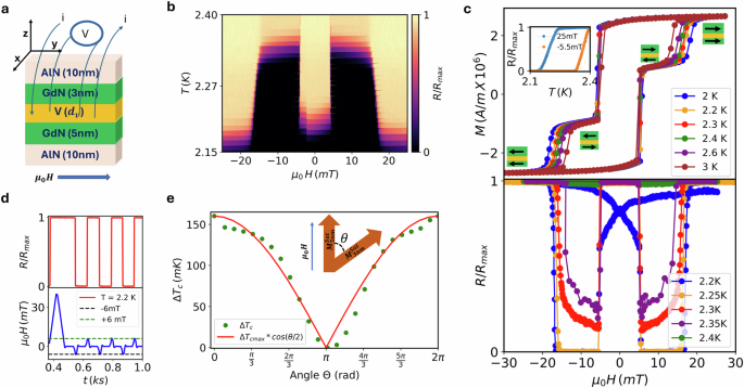
a A cartoon depiction of a typical SPSV multi-layered stack wire-bonded for four probe measurements. b Color map of 11 nm V thickness sample, where several Resistance (R) vs in plane external magnetic field (μ0H) sweeps in the sequence +25 mT to −25 mT and from −25 mT to +25 mT (termed downward and upward sweeps respectively) were performed with fixed temperatures; at 5 mK intervals from 2.15 K to 2.4 K. The color map shows the parts of MR measurements corresponding only to 0 to −25 mT, and 0 to +25 mT, from the downward and upward sweeps respectively. c Top panel shows MH loops of the 11 nm SPSV, measured at various temperatures. Inset to top panel of c shows resistance (R) vs temperature (T) measured when the relative orientation of the magnets is in P (+25 mT) and AP (−5.5 mT) configuration. Lower panel shows R vs H sweeps at various temperatures. d Demonstration of nonvolatile zero field bistable states in the 11 nm SPSV. e Measured value of \({\Delta T}_{c}\) of the 11 nm SPSV as a function of angle between saturation magnetization vectors of the two GdN layers, plotted along with an ideal \(\cos\frac{\theta }{2}\) functional behavior of \({\Delta T}_{c}\).
We note that in Fig. 1c, the transitions of the V layer into and out of the superconducting state are remarkably sharp and hence would be ideal for switching applications. Following this observation, in Fig. 1d, we show the switching characteristics of the 11 nm V trilayer over several cycles. The lower panel shows the sequence of external in-plane magnetic field application. The measurement starts with saturating both GdN layers at 40 mT, when the V layer remains in a metallic state due to P orientation of both GdN layers. Then several sequences of switching are carried out between – (+) 6 mT, thereby repeatedly achieving AP and P state of the trilayer. After application of each field, we return to zero field and record the resistance state of the device. Clear sharp transitions into and out of the superconducting state are observed at – (+) 6 mT, and interestingly the same state is retained at zero fields. This clearly demonstrates the suitability of the trilayer as a non-volatile cryogenic memory.
In Fig. 2, we show details of measurement of spin valves of several V thicknesses, and elucidate on further evidence of SEC in our system. The crux of SEC is that the onset of superconductivity in the system mediates an effective antiferromagnetic (AF) exchange interaction between the two FI layers. While the onset of superconductivity is ensured by achieving an AP state by the switching of the softer FI layer (5 nm GdN); from thereon – the superconducting state (with thickness much lower than the bulk coherence length) couples the two FI layers through coherent electrons of the cooper pair, each sitting at the top and bottom S/FI interfaces. A further experimental evidence of SEC induced AF exchange from MH and RH measurements would be that due to this new AF exchange coupling, it becomes harder than normal to come out of the AP state, and hence a higher-than-normal switching field is required to switch the 3 nm layer, in order to break out of the AP state. Through MH and RH measurements in Fig. 1c, this phenomenon is already demonstrated for the 11 nm V sample. In Fig. 2 we demonstrate this in all other measured spin valves. Since it is difficult to access MH below 2 K in most commercial magnetometers, and since the switching in RH and MH match for a sample for whom both measurements could be done for a reasonable temperature range; we base most of our observations on switching fields derived from RH measurements in color plots similar to that shown in Fig. 1b for all other SPSVs. A clear increase in switching field of the 3 nm layer is visible in the respective \(\Delta {T}_{c}\) regions; indicating that it indeed becomes harder to come out of the superconducting (AP) state. Interestingly there seems to be almost no noticeable change in the first switching fields of 5 nm GdN in all SPSVs in the \(\Delta {T}_{c}\) region. These observations are almost identical to those in the GdN/Nb/GdN system13. Please refer to Supplementary Fig. 5 for methodology adopted for choosing \(\Delta {T}_{c}\) boundaries for few SPSVs.
Fig. 2: Variation of GdN switching fields, Zeeman energy, and switching energies for various V thicknesses.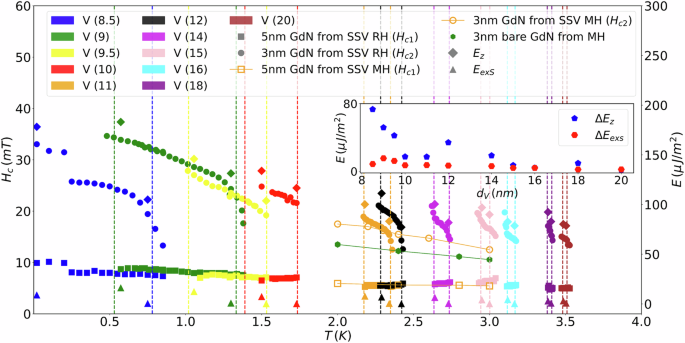
Dashed vertical lines denote the region of operation of SPSVs of various V thicknesses. All quantities of each V thickness are represented by a particular color but different shapes. Filled circles indicate switching field of 3 nm GdN from RH measurements. Unfilled circles indicate switching fields of 3 nm GdN from MH measurements. Filled squares indicate switching fields of 5 nm GdN from RH measurements. Unfilled squares indicate switching fields of 5 nm GdN from MH measurements (MH data is only available for the 11 nm sample). Filled diamonds indicate switching energy \(\left({E}_{Z}\right)\) associated with switching of the 3 nm GdN in each spin valve at the P and AP state \({T}_{c}\). Filled triangles indicate the superconducting condensation energy \(({E}_{{exS}})\) associated with the P and AP states of each spin valve. Filled hexagons indicate the switching field of a 3 nm GdN sample grown on AlN and capped by AlN.
Phenomenologically, this effect can be understood from a thermodynamical viewpoint. The onset of superconductivity in the AP state introduces the superconducting condensation energy in the system (\({E}_{{exS}}\)). For mediating the net AF exchange coupling, the increased energy for switching (\({E}_{Z}\)) of the 3 nm GdN out of the AP state to the P state must be compensated by \({E}_{{exS}}\). Hence, in the temperature range of operation of SPSVs; \({\Delta E}_{{exS}}\left({T}_{{cAP}}-{T}_{{cP}}\right)\) should be comparable to the magnitude of \({\Delta E}_{Z}\left({T}_{{cAP}}-{T}_{{cP}}\right)\). Using the expressions for the energy terms per unit area13:
$${\Delta E}_{{exS}}\left({T}_{{cAP}}-{T}_{{cP}}\right)\cong 1.5\gamma {d}_{V}{T}_{{cAP}}\left({T}_{{cAP}}-{T}_{{cP}}\right)$$
(2)
Where γ is the specific heat constant of V29 = 9.8 \({mJ}{{mol}}^{-1}{K}^{-2}\), \({d}_{V}\) is the thickness of the thin Vanadium layer, and all other terms are defined earlier.
$${\Delta E}_{Z}\left({T}_{{cAP}}-{T}_{{cP}}\right)=2{d}_{{GdN}}{M}_{{GdN}}{\mu }_{0}\left({H}_{c2-P}-{H}_{c2-{AP}}\right)$$
(3)
Where, dGdN = 3 nm, MGdN = 0.9*106 A/m, Hc2−P = 18.55 mT corresponding to switching field for 3 nm GdN at 2.18 K, and Hc2−AP = 15.39 mT corresponding to switching field of 3 nm GdN at 2.34 K.
Using the above values, we find that \({\Delta E}_{{exS}}\left({T}_{{cAP}}-{T}_{{cP}}\right)\)= 7.31 \(\mu J{m}^{-2}\), while \({\Delta E}_{Z}\left({T}_{{cAP}}-{T}_{{cP}}\right)=17.07\, \mu J{m}^{-2}\). The closeness of these two energy scales is similar to that in GdN/Nb/GdN systems13, and gives a phenomenological justification for the possibility of SEC in our system for the 11 nm SPSV. The inset to Fig. 2 shows these two energy scales plotted for all SPSVs. We note that for most of the samples these two energy scales are closely matched. For some samples especially between 8.5 and 10 nm, although there seems to be an apparent mismatch, we note that the two energy scales are roughly of the same order of magnitude.
We point out the crucial role of γ of the superconducting layer in observation of SEC, as it significantly impacts the magnitude of \({\Delta E}_{{exS}}\). Among the elemental superconductors, V has one of the highest magnitudes of \(\gamma\), and is significantly higher than that of Nb – the superconductor used for the first experimental demonstration of SEC. This was the main basis for choosing V for this experiment. It is therefore understandable why FI based SPSVs explored earlier with superconductors having almost an order of magnitude lower specific heats – Al10 (γ = 1.35 \({mJ}{{mol}}^{-1}{K}^{-2}\)) and In9 (γ = 1.67 \({mJ}{{mol}}^{-1}{K}^{-2}\)) may not show typical SEC induced AP state hardening features as shown in Fig. 2. On similar lines, we predict that among elemental superconductors, Ta with γ = 6.15 \({mJ}{{mol}}^{-1}{K}^{-2}\) and relatively high coherence length of 95 nm should be a strong contender as another alternative superconductor for observation of SEC.
Finally, we turn our attention to the possibility of realization of absolute switching using these SPSVs. The original proposal pertaining to absolute spin valve effect in CPP geometry relies on varying magnitudes of tunneling currents between two ferromagnet proximitized superconducting/metal layers separated by a tunnel barrier30. In such a device, depending on the relative orientation of the ferromagnets, a finite tunneling current appears or ideally disappears completely at the induced minigap voltage. The CIP equivalent of such a device would be the appearance or complete disappearance of the superconducting state, which is dependent on the relative orientation of ferromagnets. This phenomenon has been recently demonstrated in a EuS/Au/Nb/EuS spin valve11. Such a condition can be realized in our SPSVs if the induced exchange fields in the V layer far exceeds its superconducting gap value and well beyond the paramagnetic limit of superconductivity31,32 for V.
As indicated in previous works by Hauser9, and Li10, the P state \({T}_{c}\) of the spin valves can be used to estimate Γ and subsequently \({\overline{h}}\) for each V thickness. For estimating, \(\varGamma\) we use:
$$\frac{{T}_{{cP}}}{{T}_{c0}}=1-10\left(\frac{{\varGamma }S}{{E}_{F}}\right)\left(\frac{{\xi }_{{eff}}}{{d}_{V}}\right)$$
(4)
Where \({T}_{{cP}}\) is the P state \({T}_{c}\) for a particular Vanadium thickness (\({d}_{V}\)) spin valve, \({T}_{c0}\) is the corresponding \({T}_{c}\) of a bare V film of thickness \({d}_{V}\); \({E}_{F}\) is the fermi energy of V (approximately 10 eV) estimated using free electron theory; \({\xi }_{{eff}}\) is the zero-temperature dirty limit coherence length of each bare V film estimated from perpendicular critical field measurements shown in Supplementary Fig. 3. Figure 3a shows Γ calculated using the above equation for various V thicknesses. Using the value obtained for Γ, we use Eq. 1 to estimate the exchange field \(({\overline{h}})\) in each spin valve. While Γ fluctuates in the range of 150−250 meV, \(({\overline{h}})\) rises monotonically by more than an order of magnitude for the lowest thickness. From this observation, we expect the lowest thicknesses of V spin valves to demonstrate absolute switching. In Fig. 3b,c, we show evidence of such absolute switching in the 8.5 nm V SPSV. No evidence whatsoever of the appearance of a superconducting state is visible at the lowest temperatures till 20 mK. Finally, in Fig. 3d, we demonstrate bistable switching at 20 mK and zero field, with several different patterns of field cycling. This clearly demonstrates the suitability of application of such SPSVs for usage as sub-kelvin non-volatile memory elements.
Fig. 3: Demonstration of bistable and absolute spin switch behavior.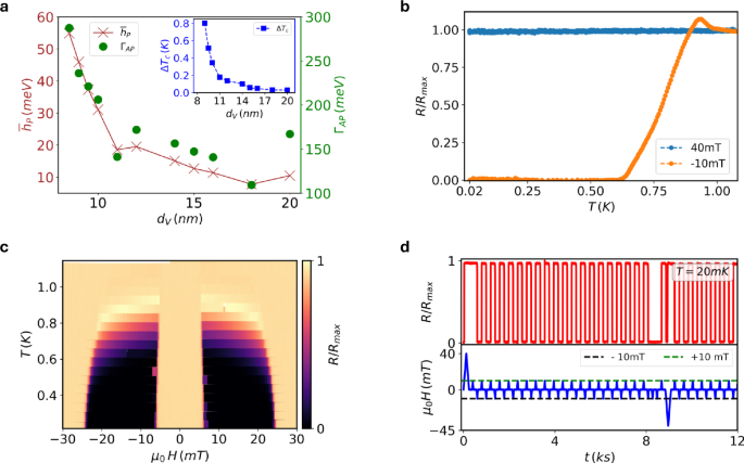
a Calculated value of exchange fields (maroon crosses) in different thicknesses of V layer SPSVs (left axes). Right axes show calculated values of the exchange constant (green circles) for every spin valve as per de Gennes formulation. Inset shows monotonic evolution of \(\Delta {T}_{c}\) with lowering of V thickness down to 9 nm. b RvsT heating measurement of the 8.5 nm SPSV with in plane external field values corresponding to P and AP states. c Color plot with RH measurements as a function of temperature for the 8.5 nm SPSV. d Demonstration of zero field bistable switching phenomena at 20 mK.
In conclusion, we have demonstrated that V-based SPSVs tally with all of de Gennes’ predictions, and it mediates SEC between FI layers. Apart from the demonstration of a new material system for observation of SEC, the highlight of this work lies in the demonstration of absolute switching and switchable bistable states at the lowest temperatures. Although evidence of bistable switching in SPSVs was shown earlier in an EuS/Al/EuS SPSV; we believe that SEC-mediated AF exchange coupled SPSVs make the non-volatile bistable states more robust and insulate them against typical field cycling effects related to domain wall dynamics and minor loop magnetization changes33. Moreover, switching in these SPSVs is remarkably sharp and hence well-suited for practical applications as cryogenic memory devices.